Abstract:
Using the Physical Vapor Transport (PVT) method, we grew a 4H-SiC single crystal with a diameter of 209 mm through a diameter-expanding technique. Subsequently, we fabricated the 8-inch SiC single crystal substrate by employing multi-wire cutting, grinding, polishing, and other processes.
To evaluate the crystal structure, crystallinity, micropipe density, resistivity, stress, surface profile, and dislocation density of the 8-inch substrate, we applied a series of characterization techniques. These techniques included Raman spectroscopy, high-resolution X-ray diffraction, optical microscopy, resistivity measurement, polarization stress measurement, surface profile measurement, and dislocation detection.
Raman spectroscopy showed that 100% of the 8-inch SiC substrate area consisted of a single 4H crystal type. Moreover, the full width at half maximum (FWHM) of the five-point X-ray rocking curve of the (004) plane ranged from 10.44″ to 11.52″.
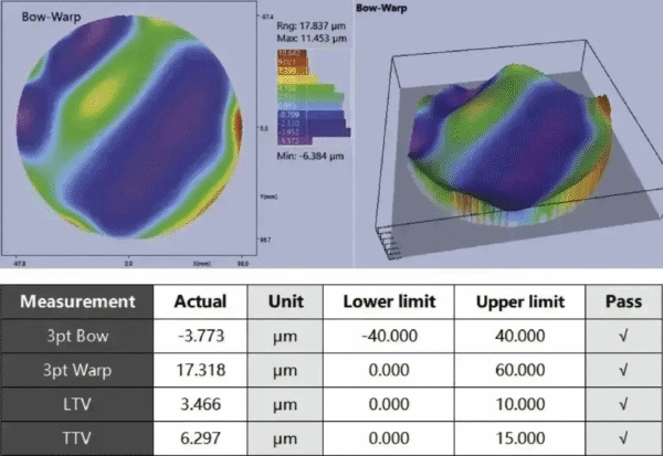
In addition, we found the average micropipe density to be 0.04 cm^-2, while the average resistivity measured 0.0203 Ω·cm. Polarization stress measurements indicated that the stress distribution across the 8-inch SiC substrate was uniform, with no areas of stress concentration detected. Furthermore, we recorded the warp at 17.318 μm and the bow at -3.773 μm.
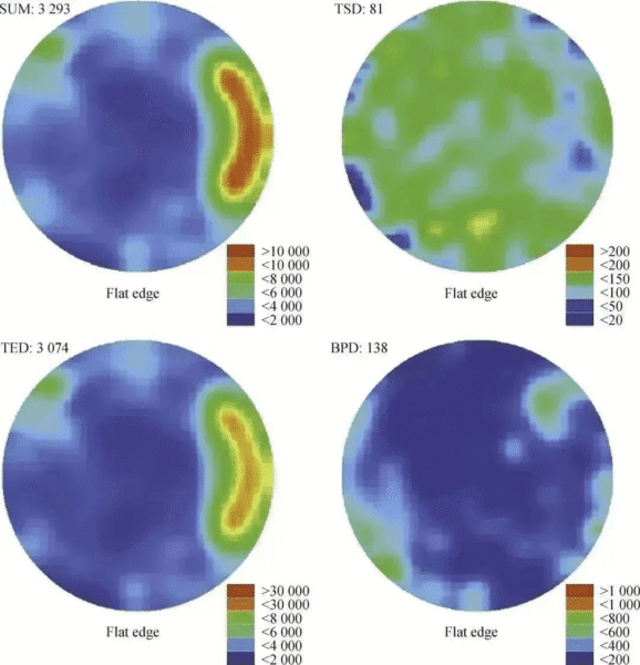
After performing 540 °C molten KOH etching, we measured the dislocation density of the 8-inch substrate using an automatic dislocation density scanner. The results indicated that the average total dislocation density measured 3293 cm^-2, with screw dislocation (TSD) density at 81 cm^-2, edge dislocation (TED) density at 3074 cm^-2, and basal plane dislocation (BPD) density at 138 cm^-2.
These results clearly demonstrate that the 8-inch conductive 4H-SiC substrate meets the advanced industry standards, confirming its suitability for high-performance applications.
Keywords: 8-inch SiC single crystal substrate; Physical Vapor Transport method; X-ray rocking curve; micropipe density; warp and bow; dislocation density
1. Introduction
Silicon carbide (SiC) is a third-generation semiconductor material. It offers several advantages, such as a wider bandgap, higher breakdown field, and higher thermal conductivity. These properties make SiC ideal for high-temperature, high-voltage, and high-frequency applications. As a result, SiC has become one of the main development directions in the semiconductor material technology field.
SiC substrates can be divided into two main types: conductive and semi-insulating.
These types differ in terms of epitaxial layers and downstream applications. Conductive SiC substrates undergo homoepitaxial growth and device fabrication. Manufacturers use them to produce power devices, such as SiC diodes and metal-oxide-semiconductor field-effect transistors (MOSFETs). These devices find widespread use in new energy vehicles, photovoltaic power generation, rail transportation, smart grids, and aerospace. On the other hand, semi-insulating SiC substrates undergo gallium nitride (GaN) epitaxy and device fabrication. Manufacturers use them to make high electron mobility transistors (HEMTs), which find applications in microwave and radio frequency devices, especially in 5G communications, satellites, and radar.
In the semiconductor industry chain, the substrate serves as the foundation for wafer manufacturing. It acts as the base material for all semiconductor chips. The substrate is crucial for physical support, heat dissipation, and electrical conduction. Specifically, in SiC power semiconductor devices, the quality of the SiC substrate directly influences the quality of the epitaxial material. This, in turn, determines the performance of the SiC power devices.
Achieving high-quality SiC substrates presents two main challenges: crystal growth and processing. SiC usually requires high-temperature (>2000 °C) growth conditions. Furthermore, SiC has over 250 crystal forms. This makes creating high-quality single-phase crystals both costly and difficult. Additionally, the hardness of SiC is close to that of diamond. This makes processing single crystals very challenging and expensive.
Studies have shown that substrate costs represent nearly 50% of the total cost in SiC device manufacturing. Larger substrates enable manufacturers to integrate more chips per wafer, which ultimately lowers the cost per chip. For instance, using an 8-inch substrate lets manufacturers cut nearly 90% more chips compared to a 6-inch wafer. It also reduces edge waste by 7%, thus lowering chip costs. Therefore, increasing substrate size is one of the main methods for reducing costs and improving efficiency in the SiC industry chain.
Currently, 6-inch substrates dominate the SiC substrate market. However, 8-inch substrates are considered a major direction for the development of SiC semiconductors. In 2015, Wolfspeed Inc. (formerly Cree), the industry leader, first demonstrated 8-inch SiC samples. Other companies, such as Coherent Corp. (formerly II-VI Inc.), Rohm Semiconductor Co. Ltd., and STMicroelectronics, have also announced the development of 8-inch SiC substrates.
Wolfspeed Inc. is currently the only company mass-producing 8-inch SiC substrates. Its 8-inch SiC substrate factory in Mohawk Valley, New York, began production in April 2022. While the domestic industry and research institutions started later, they have made significant progress. In 2022, several institutions, such as Guangdong Vastron Technology Co., Ltd, Institute of Physics, Chinese Academy of Sciences, Shanxi ShuoKe Crystal Co., Ltd., Shandong Tianyue Advanced Materials Technology Co., Ltd., and Shandong University, announced the successful development of 8-inch products.
Guangdong Vastron Technology Co., Ltd, founded in 2006, is the first domestic high-tech enterprise specializing in the R&D and industrialization of SiC single crystal substrates.
Guangdong Vastron Technology Co., Ltd has focused on the SiC substrate sector for over a decade. Its 6-inch SiC substrate products are now mass-produced and widely recognized by renowned semiconductor device companies. In 2020, Guangdong Vastron Technology Co., Ltd began working on the R&D of 8-inch conductive SiC single crystal substrates. After more than two years of hard technical work, the company overcame key challenges in 8-inch crystal diameter expansion growth and wafer processing. As a result, the company successfully fabricated high-quality 8-inch conductive SiC single crystal substrates. The company plans to achieve small-scale mass production in 2023.
The same product that we can offer
2. Experiment
Silicon carbide (SiC) is a third-generation semiconductor material. It offers several advantages, such as a wider bandgap, higher breakdown field, and higher thermal conductivity. These properties make SiC ideal for high-temperature, high-voltage, and high-frequency applications. As a result, SiC has become one of the main development directions in the semiconductor material technology field.
Manufacturers divide SiC substrates into two main types: conductive and semi-insulating.
These types differ in terms of epitaxial layers and downstream applications. Manufacturers use conductive SiC substrates for homoepitaxial growth and device fabrication. They produce power devices, such as SiC diodes and metal-oxide-semiconductor field-effect transistors (MOSFETs). These devices have widespread applications in new energy vehicles, photovoltaic power generation, rail transportation, smart grids, and aerospace. On the other hand, manufacturers use semi-insulating SiC substrates for gallium nitride (GaN) epitaxy and device fabrication. They make high electron mobility transistors (HEMTs), which find applications in microwave and radio frequency devices, especially in 5G communications, satellites, and radar.
In the semiconductor industry chain, the substrate serves as the foundation for wafer manufacturing. It acts as the base material for all semiconductor chips. The substrate plays a crucial role in providing physical support, heat dissipation, and electrical conduction. Specifically, in SiC power semiconductor devices, the quality of the SiC substrate directly influences the quality of the epitaxial material. This, in turn, determines the performance of the SiC power devices.
Achieving high-quality SiC substrates presents two main challenges: crystal growth and processing. SiC typically requires high-temperature (>2000 °C) growth conditions. Furthermore, SiC has over 250 crystal forms, which makes it difficult and costly to create high-quality single-phase crystals. Additionally, the hardness of SiC is close to that of diamond, which makes processing single crystals very challenging and expensive.
Studies show that substrate costs represent nearly 50% of the total cost in SiC device manufacturing. Larger substrates enable manufacturers to integrate more chips per wafer, which, in turn, ultimately lowers the cost per chip. For instance, using an 8-inch substrate allows manufacturers to cut nearly 90% more chips compared to a 6-inch wafer. This, in turn, reduces the overall cost. Additionally, it reduces edge waste by 7%, thereby lowering chip costs. Therefore, increasing substrate size becomes one of the main methods for reducing costs and improving efficiency in the SiC industry chain.
Currently, 6-inch substrates dominate the SiC substrate market. However, 8-inch substrates have emerged as a major direction for the development of SiC semiconductors. In 2015, Wolfspeed Inc. (formerly Cree), the industry leader, first demonstrated 8-inch SiC samples. Other companies, such as Coherent Corp. (formerly II-VI Inc.), Rohm Semiconductor Co. Ltd., and STMicroelectronics, have also announced the development of 8-inch SiC substrates.
Wolfspeed Inc. currently leads the mass production of 8-inch SiC substrates. Its 8-inch SiC substrate factory in Mohawk Valley, New York, began production in April 2022. Although the domestic industry and research institutions started later, they have made significant progress. In 2022, several institutions, including Guangdong Vastron Technology Co., Ltd., Institute of Physics, Chinese Academy of Sciences, Shanxi ShuoKe Crystal Co., Ltd., Shandong Tianyue Advanced Materials Technology Co., Ltd., and Shandong University, announced the successful development of 8-inch products.
Guangdong Vastron Technology Co., Ltd., founded in 2006, stands as the first domestic high-tech enterprise specializing in the R&D and industrialization of SiC single crystal substrates.
Guangdong Vastron Technology Co., Ltd. has focused on the SiC substrate sector for over a decade. Its 6-inch SiC substrate products are now mass-produced and widely recognized by renowned semiconductor device companies. In 2020, Guangdong Vastron Technology Co., Ltd. began working on the R&D of 8-inch conductive SiC single crystal substrates. After more than two years of hard technical work, the company overcame key challenges in 8-inch crystal diameter expansion growth and wafer processing. As a result, the company successfully fabricated high-quality 8-inch conductive SiC single crystal substrates. The company plans to achieve small-scale mass production in 2023.
pany successfully fabricated high-quality 8-inch conductive SiC single crystal substrates. The company plans to achieve small-scale mass production in 2023.
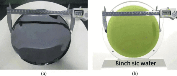
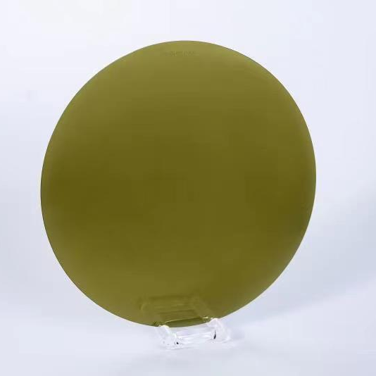
Figure 1: 8-inch SiC Crystal Ingots and Wafers. (a) SiC crystal ingot with a diameter of 209 mm; (b) standard 8-inch SiC wafer.
The Raman spectroscopy results for the 357 test points on the wafer are shown in Figure 2. All test points displayed Raman peaks with similar morphology, and the deviation from the phonon mode and the simplified wave vector and symmetry of the Raman peak at 204 cm⁻¹ (FTA, x=0.5, E2) did not exceed 0.65 cm⁻¹. Meanwhile, no high-intensity simplified wave vector modes corresponding to the 6H crystal type FTA mode (150 cm⁻¹) or the 15R crystal type FTA mode (174 cm⁻¹) were detected in the results . Therefore, it can be concluded that the 4H crystal type accounts for 100% of the 8-inch SiC wafer.
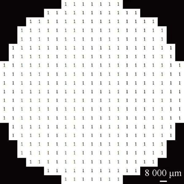
Figure 2: Raman Spectroscopy Scan of 8-inch 4H-SiC Wafer (1 for 4H-SiC, 2 for 6H-SiC, 3 for 15R-SiC).
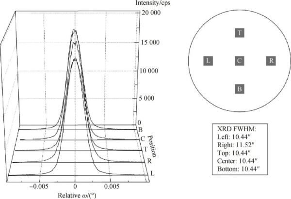
The high-resolution X-ray rocking curve test results are shown in Figure 3, with the test points located at the center of the substrate and at the central positions of the top, bottom, left, and right radii, totaling five points. From the figure, it can be seen that the (004) diffraction peaks at all test points are single peaks, and the full width at half maximum (FWHM) ranges from 10.44″ to 11.52″. This indicates that the crystallinity of the 8-inch 4H-SiC substrate is excellent, with no defects such as polycrystals or small-angle grain boundaries that would affect the crystallization quality.
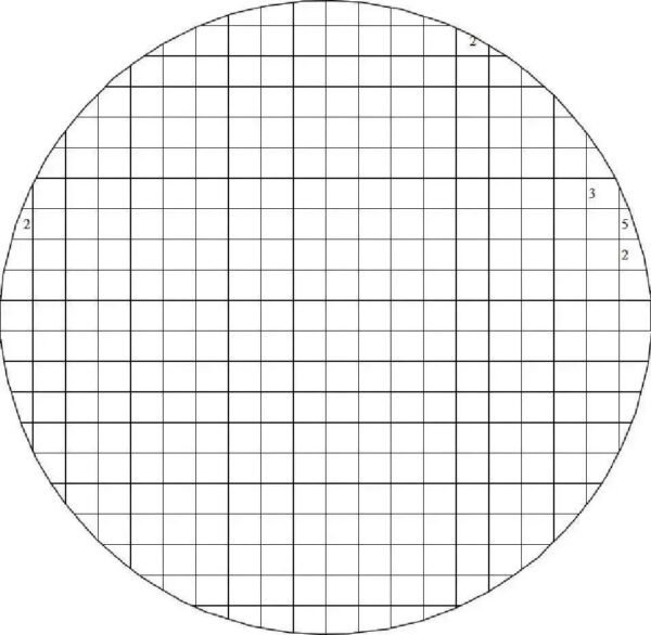
We conducted an automatic scan of the micropipe density on the 8-inch substrate using an optical microscope. After removing the micropipes from the 3 mm edge area for statistical analysis, we found that the micropipe density of the 8-inch substrate measured 0.04 cm⁻². In total, we observed 14 micropipes across the entire substrate. Notably, all of these micropipes were concentrated at the edges, as shown in Figure 4. This distribution pattern suggests that the majority of micropipes occur near the peripheral regions of the substrate, which may indicate challenges related to the growth conditions or edge processing.
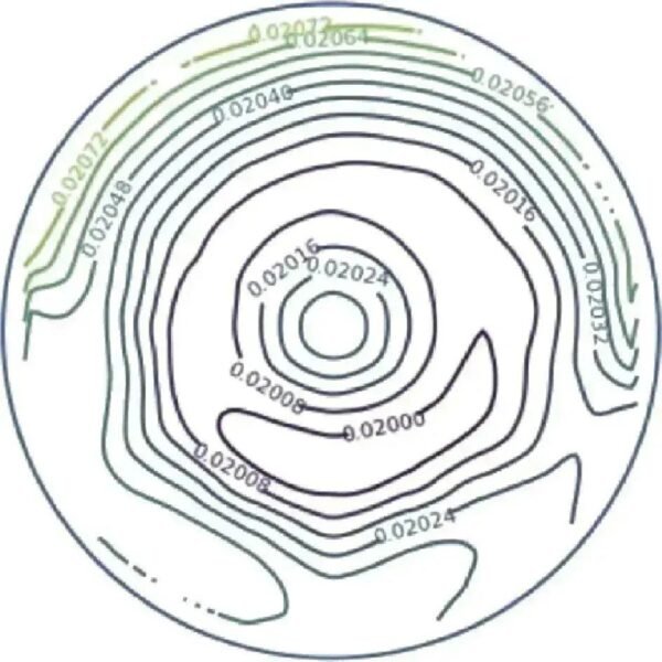
The resistivity of the 8-inch SiC substrate was tested using the non-contact eddy current method, with the results shown in Figure 5. The results indicate that the average resistivity of the 8-inch substrate is 0.0203 Ω·cm, with a maximum value of 0.0208 Ω·cm, a minimum value of 0.0199 Ω·cm, and a relative standard deviation of 1.11%
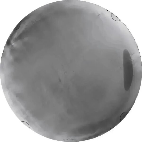
The stress distribution of the 8-inch substrate detected using the polarization stress meter is shown in Figure 6. Generally, regions with significant light and dark fluctuations in the test results indicate higher stress [9]. The overall stress distribution of the 8-inch SiC substrate is uniform, with low-intensity stress regions found only at the outer edges of the small face and along the substrate edge. Most areas show no significant stress concentration, indicating good crystallization quality of the crystal.