

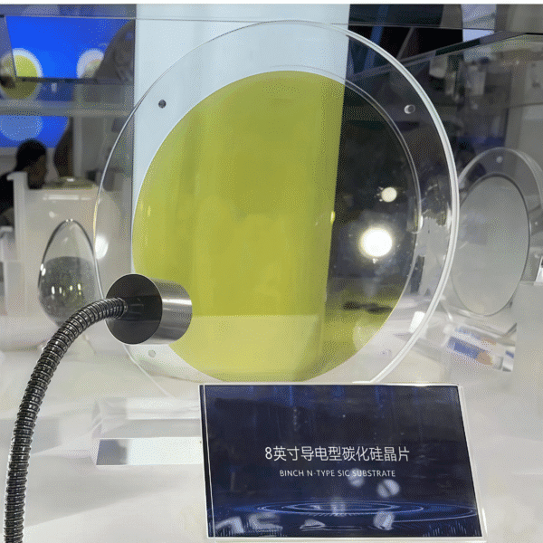
8-Inch 4H-N SiC Wafer – Prime Grade Substrate for Next-Generation Power Electronics
Introduction
The global semiconductor industry keeps evolving because new applications demand higher efficiency, smaller device sizes, and stronger thermal stability. Traditional silicon wafers reach their physical limits when engineers design devices that work at high voltage and high temperature. As a result, many companies adopt SiC wafer as the core material for next-generation devices.
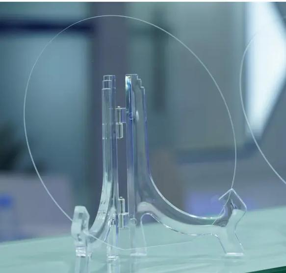
The 8-inch 4H-N SiC wafer represents the future of power electronics because it combines wide bandgap properties, high electron mobility, and strong mechanical strength. Manufacturers and research institutes across the world now focus on Prime Grade 8-inch wafers since they reduce production costs and improve device yield. Moreover, the transition from 6-inch to 8-inch wafers allows large-scale fabrication, which accelerates commercialization in electric vehicles, renewable energy, and communication systems.
Product Overview
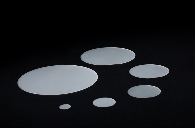
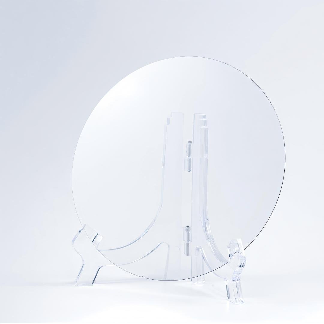
We provide Prime Grade 8-inch 4H-N SiC wafer with excellent crystal quality and low defect density. These wafers ensure consistent performance for epitaxial growth, device fabrication, and mass production. Because they meet strict specifications, they support both high-volume industrial manufacturing and advanced research projects.
The 4H polytype remains the most important structure because it offers superior electron transport, high critical electric field, and efficient thermal conductivity. With these features, 8-inch sic wafer products provide an ideal platform for MOSFETs, diodes, and advanced optoelectronic devices.
Technical Specifications
The specifications of our 8-inch SiC wafer guarantee reliability and reproducibility. Each parameter contributes to higher device yield and stable performance:
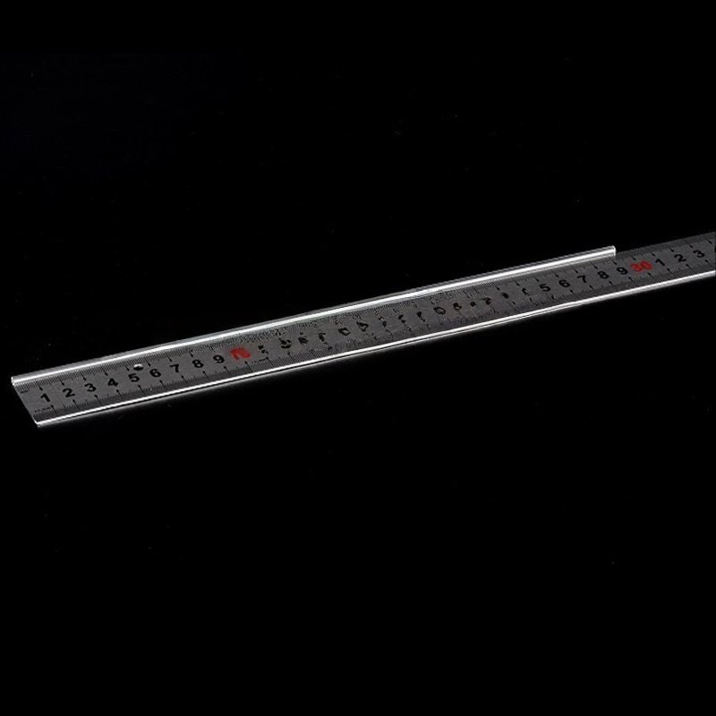
Diameter: 199.5 mm – 200.0 mm.
Polytype: 4H, designed for superior electron mobility.
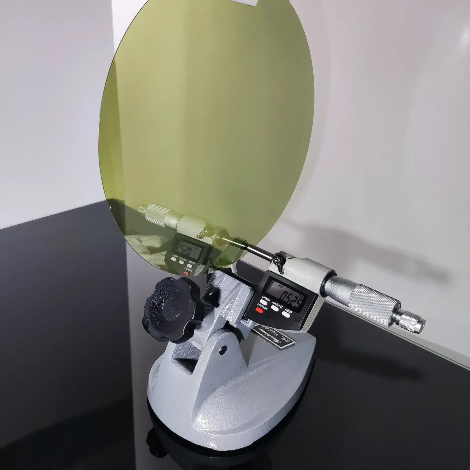
Thickness: 500 µm ± 25 µm, offering mechanical strength for processing.
Wafer Orientation: 4° off-axis toward <11-20> ± 0.5°, suitable for epitaxial growth.
Micropipe Density: ≤ 0.2 cm⁻², which ensures reliable large-area devices.
Resistivity: 0.015 – 0.025 Ω·cm, providing uniform doping control.
Notch Orientation: (10-10) ± 5.0°.
Edge Exclusion: 3 mm.
LTV / TTV / Bow / Warp: ≤ 5 µm / 10 µm / 35 µm / 70 µm.
Roughness: Polished Ra ≤ 1 nm, CMP Ra ≤ 0.2 nm.
Defect Control:
Edge cracks eliminated by high intensity light inspection.
Hex pits controlled with cumulative area ≤ 0.05%.
Polytype inclusions controlled with cumulative area ≤ 0.05%.
Visual carbon inclusions removed.
Scratches and chips tightly limited to ≤ 0.2 mm in width and depth.
Threading screw dislocation ≤ 3,000 cm⁻².
No silicon contamination detected by high intensity inspection.
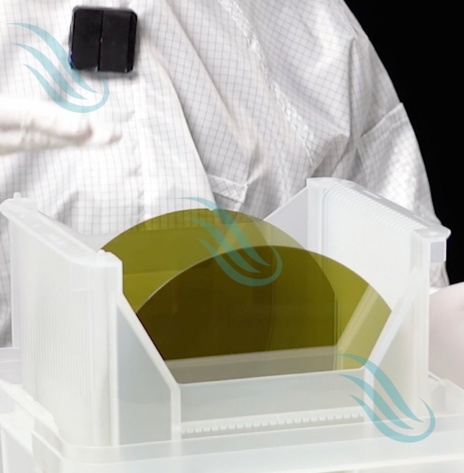
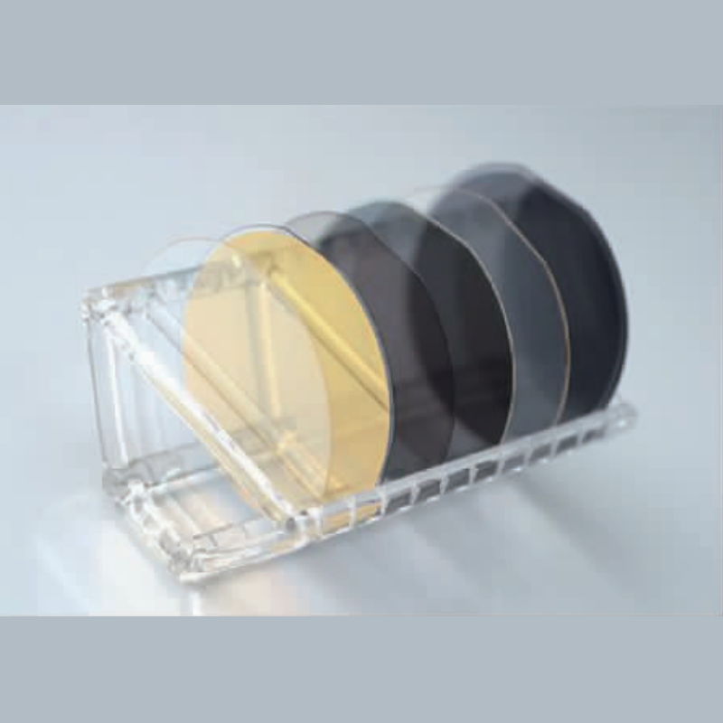
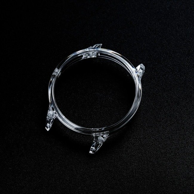
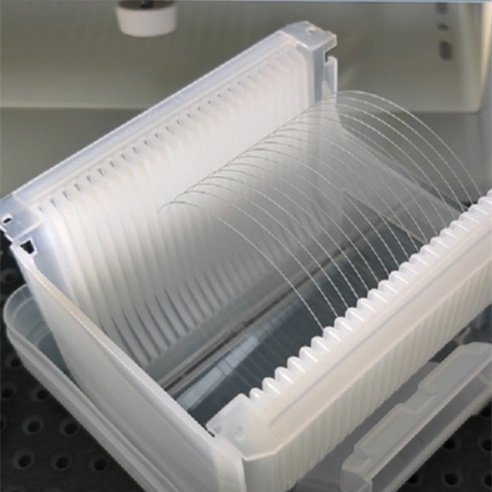
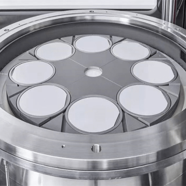
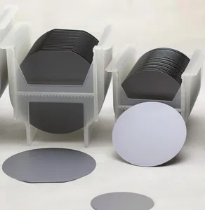
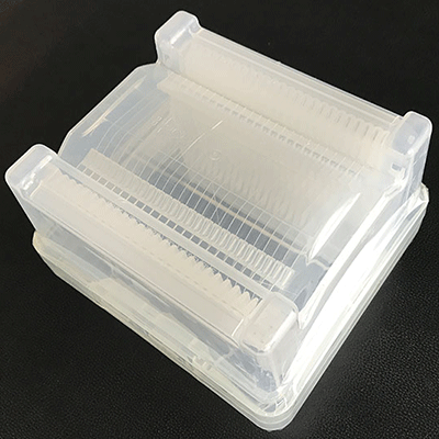
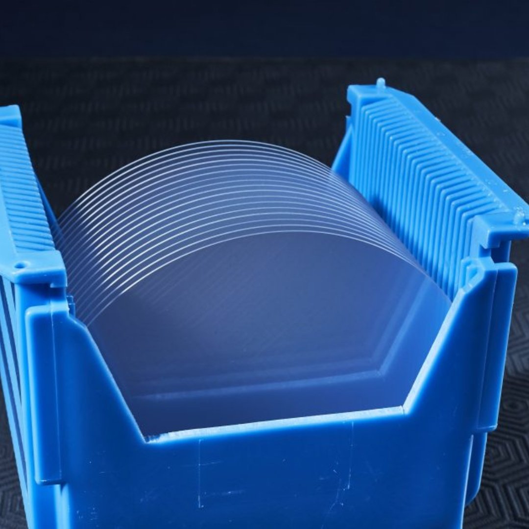
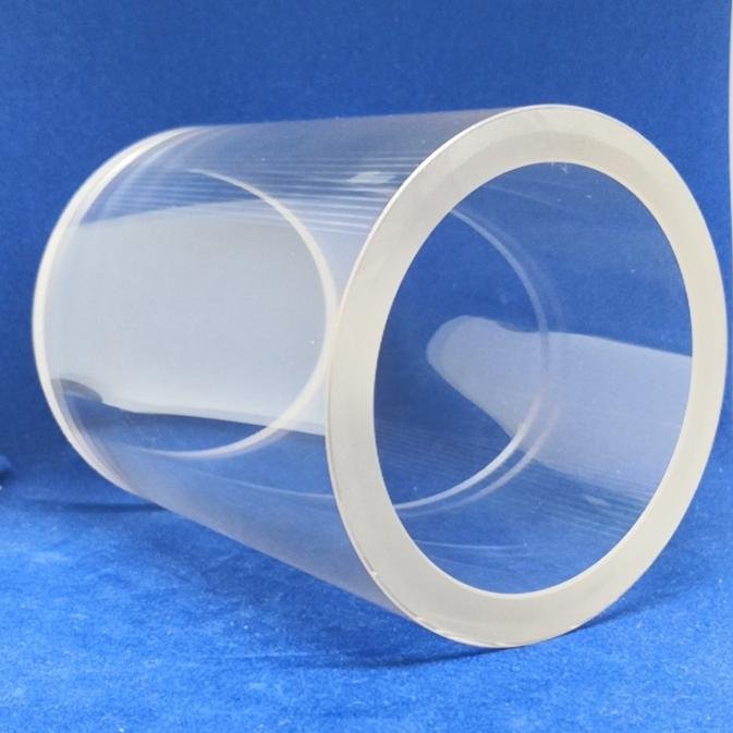
Packaging: Multi-wafer cassette or single wafer container, ensuring safe global transport.
Because of these specifications, customers benefit from consistent wafer quality and predictable device output.
Grade Options: Z Grade vs Dummy Grade
We offer two categories of 8-inch wafers to satisfy different needs:
Zero MPD Production Grade (Z Grade)
Micropipe density ≤ 0.2 cm⁻².
Low defect density guarantees high device yield.
Perfect for epitaxy and large-scale device production.
Stable parameters ensure reproducibility across batches.
Dummy Grade (D Grade)
Designed for process development and equipment calibration.
Cost-effective solution for laboratories and pilot runs.
Suitable for etching tests, coating evaluation, and training.
Provides consistent surface quality at lower cost.
Because industrial customers often require both R&D and production, combining Z Grade wafers with Dummy Grade wafers creates an efficient workflow.
Advantages of Our 8-Inch SiC Wafer
Choosing our Prime Grade sic wafer brings multiple benefits:
High Quality: Tight control of dislocations, micropipes, and scratches.
Excellent Flatness: LTV, TTV, and warp values remain extremely low, which supports precise lithography.
Superior Surface Quality: CMP Ra ≤ 0.2 nm, ideal for epitaxial deposition.
Thermal Conductivity: High thermal capacity ensures reliable device operation at elevated temperature.
Scalability: 8-inch diameter reduces cost per device because more chips fit on one wafer.
Global Standards: Specifications align with international benchmarks, which makes integration easier.
Moreover, our wafers allow manufacturers to achieve higher energy efficiency and lower power loss in devices. Therefore, they accelerate the adoption of wide bandgap semiconductors in multiple industries.
Applications
The 8-inch sic wafer enables innovation across many sectors:
Electric Vehicles: On-board chargers, inverters, and DC/DC converters demand high voltage and high frequency devices.
Renewable Energy: Solar inverters and wind power systems require reliable wide bandgap substrates.
Power Grids: High-voltage switches and converters depend on robust 8-inch wafers.
5G and Communication: High-frequency devices rely on low defect substrates.
Industrial Equipment: Motor drives and automation systems gain efficiency with SiC devices.
Optoelectronics: GaN-on-SiC epitaxy improves LED and RF performance.
Because these markets continue to expand, the demand for Prime Grade 8-inch wafers grows steadily.
Packaging and Delivery
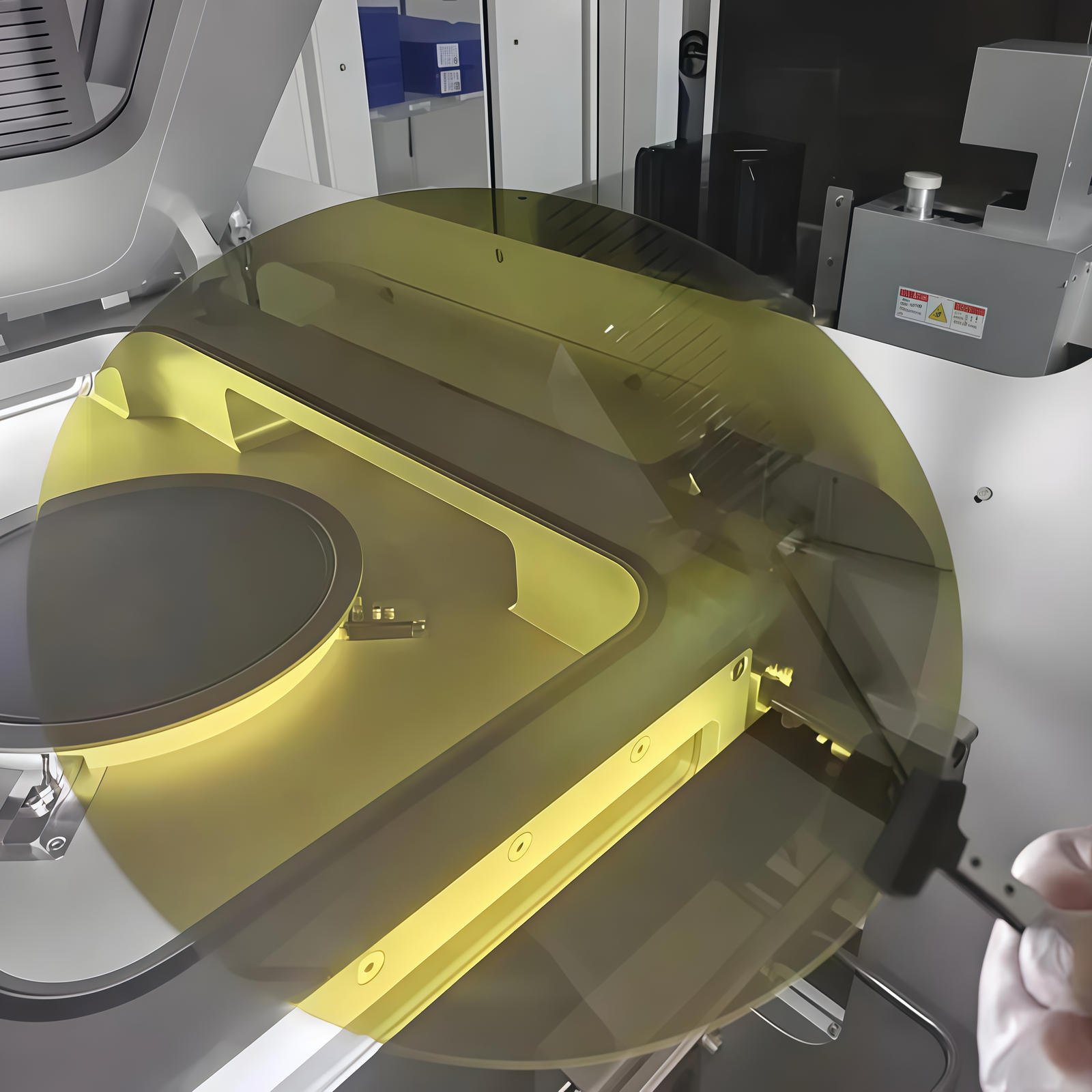
Every wafer is packaged in a cleanroom environment. We use multi-wafer cassettes or single wafer containers depending on order size. In addition, each container protects wafers from contamination, vibration, and mechanical damage. Because safe delivery remains critical, we cooperate with trusted logistics partners to ship worldwide on schedule.
Conclusion and Call to Action
The 8-inch Prime Grade 4H-N SiC wafer stands at the center of the wide bandgap revolution. With tight specifications, superior surface quality, and stable global supply, our wafers support both high-volume production and advanced R&D.
If you need sic wafer solutions for next-generation devices, contact our sales team today. We provide fast quotations, technical consultation, and reliable international shipping. Because your success depends on strong materials, we dedicate ourselves to delivering wafers that help you lead in the global semiconductor market.