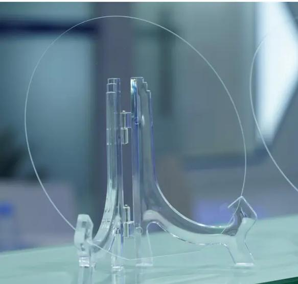

6-inch SiC Semi-insulating Wafer | Zero MPD Production Grade
Why Choose Semi-insulating SiC Wafers
Semi-insulating silicon carbide (SiC) wafers are the foundation of next-generation RF, microwave, and high-power electronic devices. Compared with traditional substrates, they not only provide higher resistivity but also ensure excellent thermal conductivity and outstanding flatness. Therefore, they have become the preferred choice for RF power amplifiers, 5G communication systems, and other advanced technologies.
Moreover, since the demand for Zero Micropipe Density (Zero MPD) wafers continues to increase, manufacturers are facing stricter quality requirements. Consequently, semi-insulating SiC wafers are not only gaining wider recognition but also becoming the most reliable option for achieving stable and consistent performance in demanding device manufacturing. Therefore, many industries now prefer SiC semi-insulating wafers as the foundation for next-generation applications.
Key Technical Specifications
| Parameter | Specification |
|---|---|
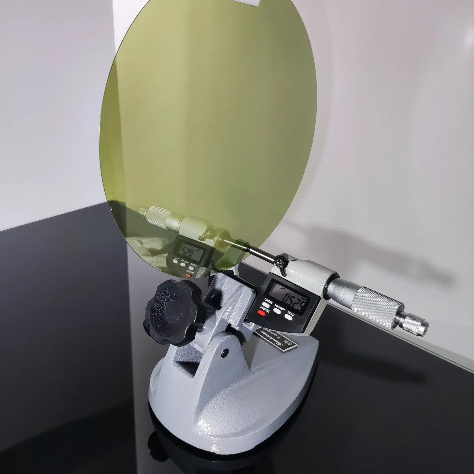
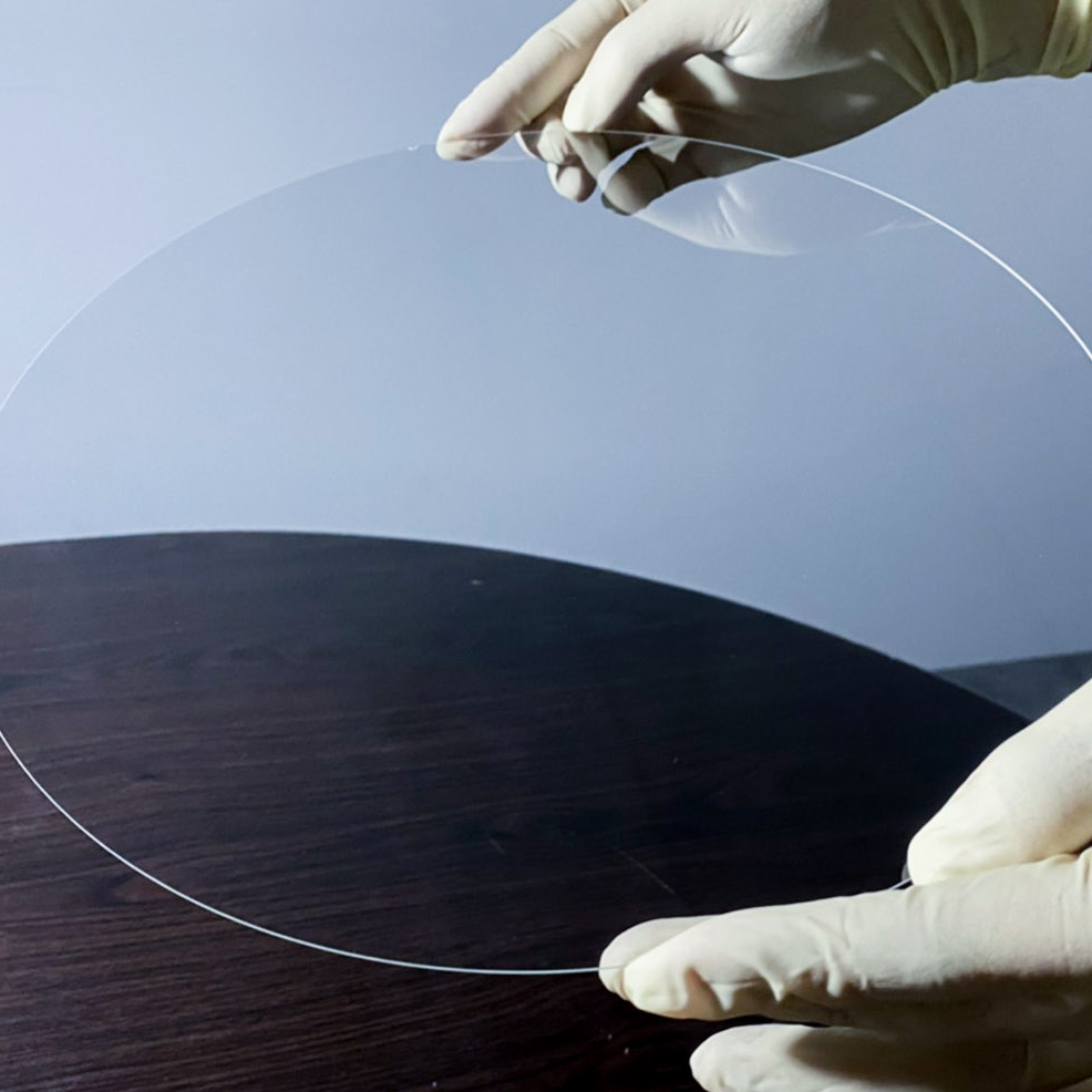
| Diameter | 149.5 mm – 150.0 mm |
| Thickness | 500 μm ± 15 μm |
| Grade Options | Z Grade (Zero MPD Production) / D Grade (Dummy) |
| Poly-type | 4H |
| Orientation | On axis <0001> ± 0.5° |
| Micropipe Density (MPD) | ≤ 1 cm⁻² |
| Resistivity | ≥ 1E10 Ω·cm |
| Primary Flat Orientation | {10-10} ± 5.0° |
| Flatness Control (LTV / TTV) | ≤ 2.5 μm / ≤ 6 μm |
| Bow / Warp | ≤ 25 μm / ≤ 35 μm |
| Surface Roughness (Polish) | Ra ≤ 1 nm |
| Surface Roughness (CMP) | Ra ≤ 0.2 nm |
| Carbon Inclusion (Visual) | ≤ 0.05% cumulative area |
| Edge Chips | None permitted ≥ 0.2 mm width and depth |
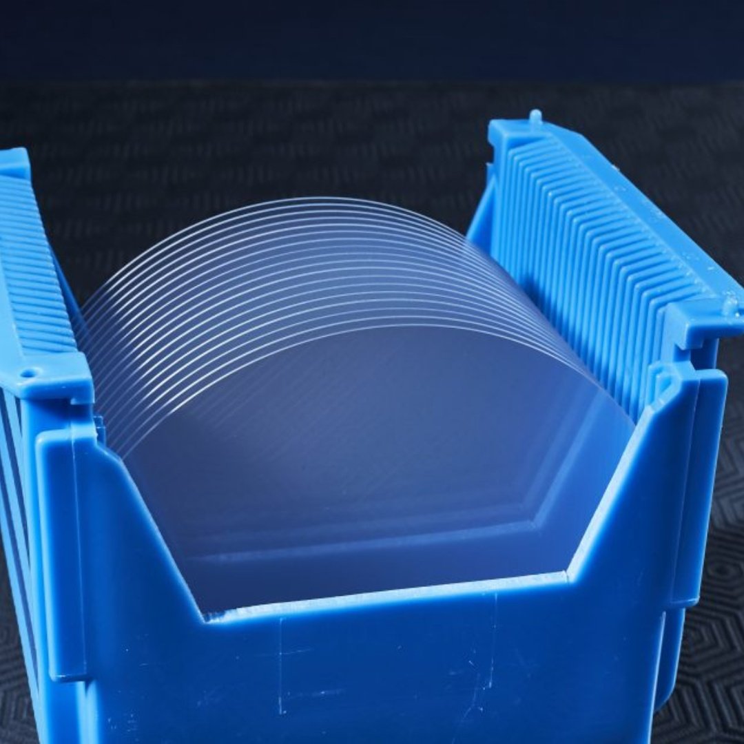
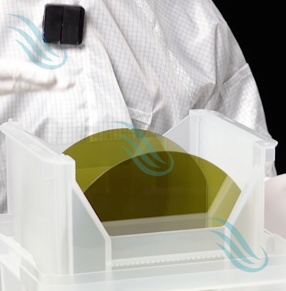
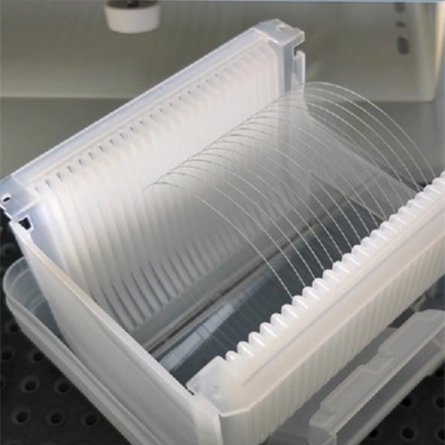
| Packaging | Multi-wafer cassette / Single-wafer container |
Because of these strict parameters, wafers achieve exceptional performance consistency. Furthermore, they reduce production risks and improve downstream device efficiency.
Manufacturing Achievements and Process Control
To guarantee top-tier wafer quality, advanced process control methods are applied throughout manufacturing. For example, micropipe-free density control enables Zero MPD standards, while monocrystalline growth control ensures structural integrity.
In addition, resistivity regulation techniques guarantee stable device operation. Furthermore, inclusion and impurity control minimize structural defects and improve long-term reliability. At the same time, substrate step width and flatness optimization ensure full compatibility with subsequent processing stages. Therefore, manufacturers can achieve higher production yields and more consistent device quality.
As a result, semi-insulating SiC wafers deliver not only excellent uniformity but also ultra-high resistivity and minimal surface defects. Consequently, they represent an ideal choice for advanced RF, microwave, and high-power applications.
Applications of SiC Semi-insulating Wafers
Thanks to their unique electrical and structural properties, semi-insulating SiC wafers are used in a wide range of fields:
RF Power Devices – including RF amplifiers, low-noise amplifiers, and high-frequency switches.
5G Communication Systems – ensuring stable signal transmission and lower energy loss.
Microwave Devices – for radar, satellite communication, and aerospace electronics.
High-Power Electronics – improving efficiency in power management and conversion.
Research & Development – serving as substrates for novel semiconductor and quantum devices.
Therefore, SiC semi-insulating wafers are not only ideal for high-performance industrial applications but also critical in next-generation communication and defense technologies.
Packaging and Delivery
Every wafer is packaged with reliability in mind. Customers can choose between multi-wafer cassettes or single-wafer containers. Consequently, this packaging approach ensures safe handling, minimizes contamination, and supports efficient storage.
Customization Available
In conclusion, 6-inch semi-insulating SiC wafers combine Zero MPD grade, ultra-high resistivity, and advanced defect control. Therefore, they provide a reliable solution for RF, 5G, and high-frequency electronic devices.
👉 We also offer customized wafer specifications according to customer requirements, including diameter, thickness, resistivity, and orientation. Please contact us to discuss tailored solutions that meet your project needs.