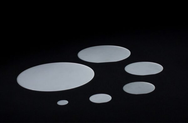

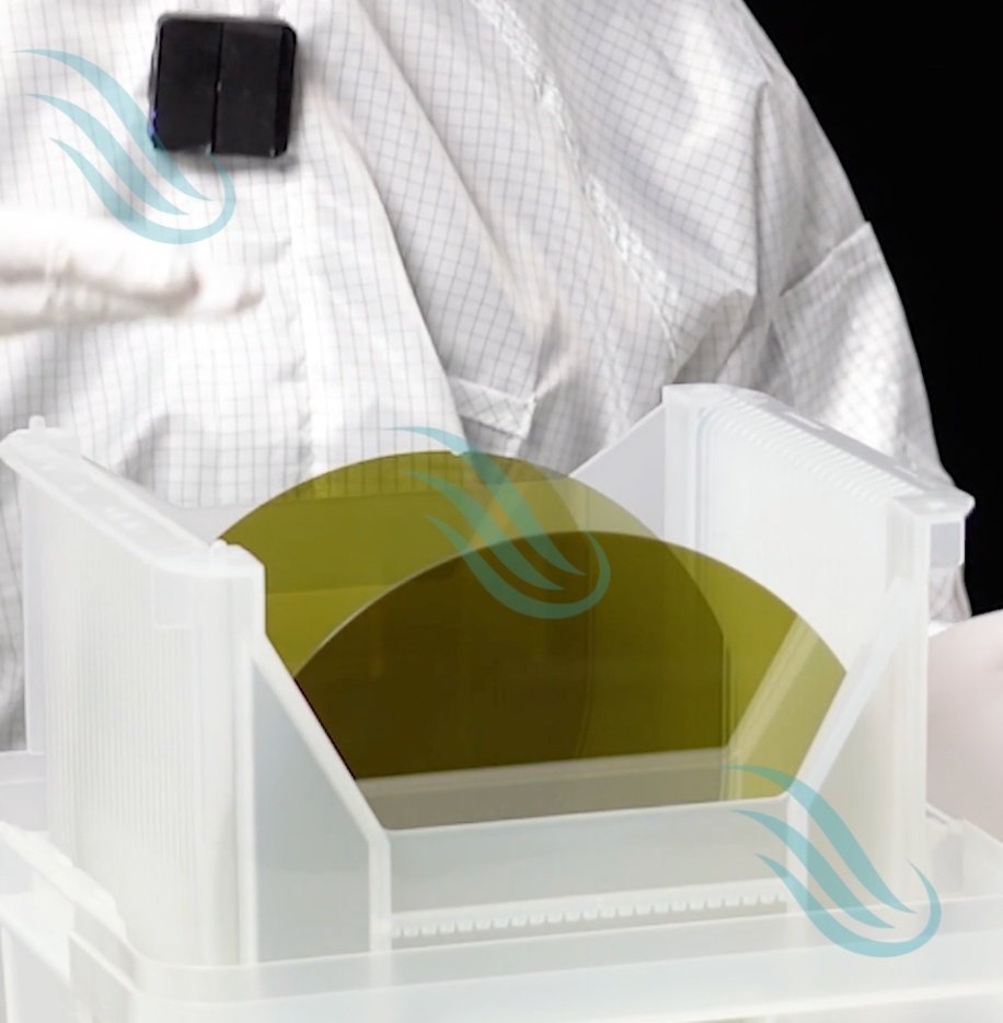
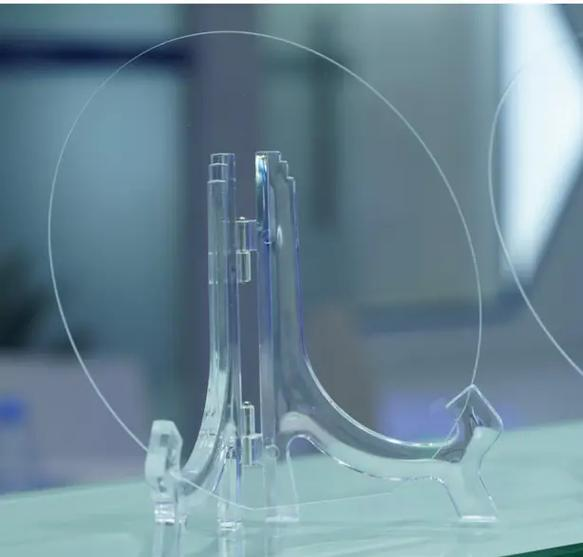
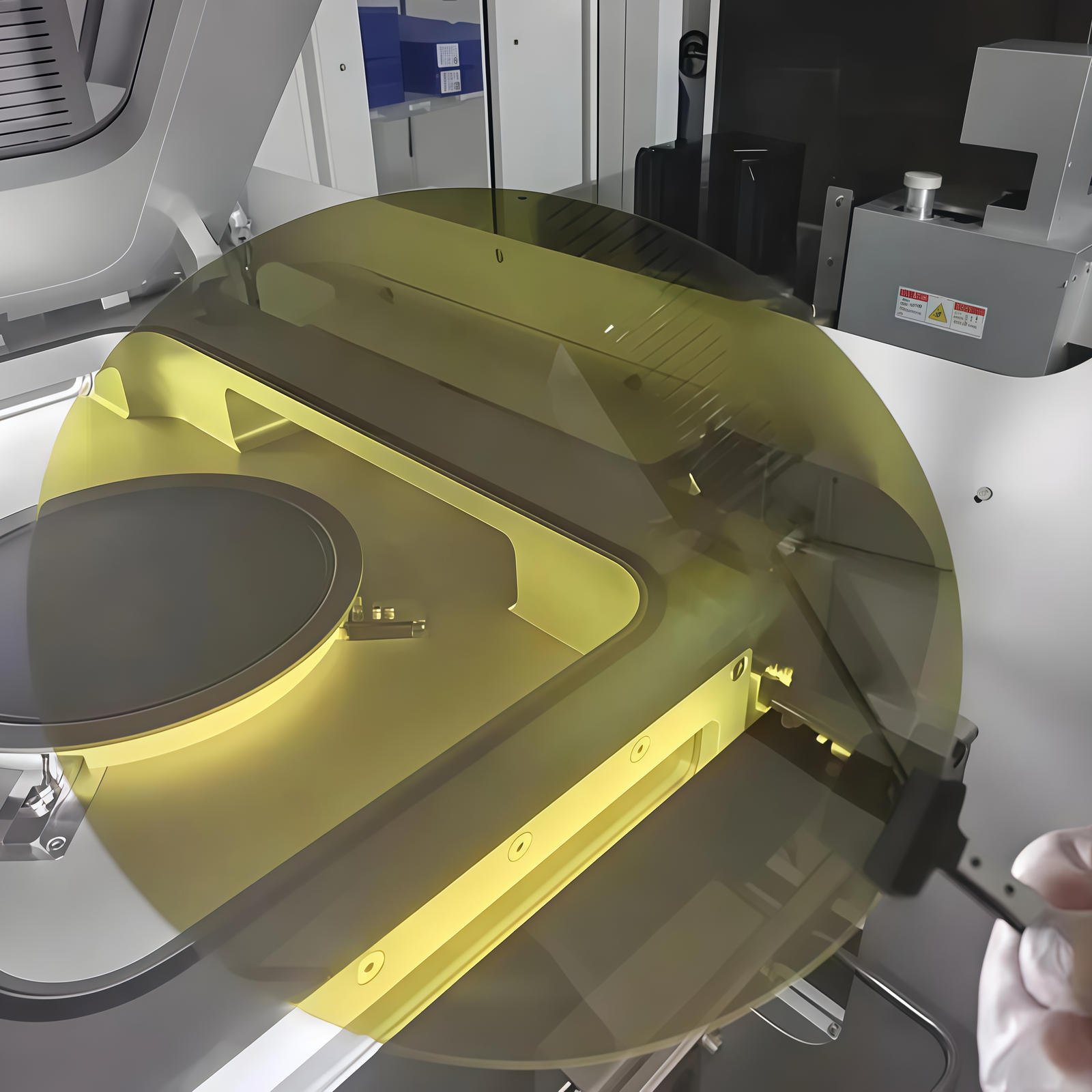
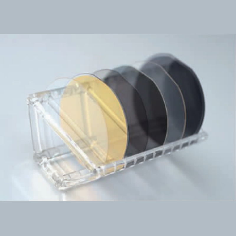
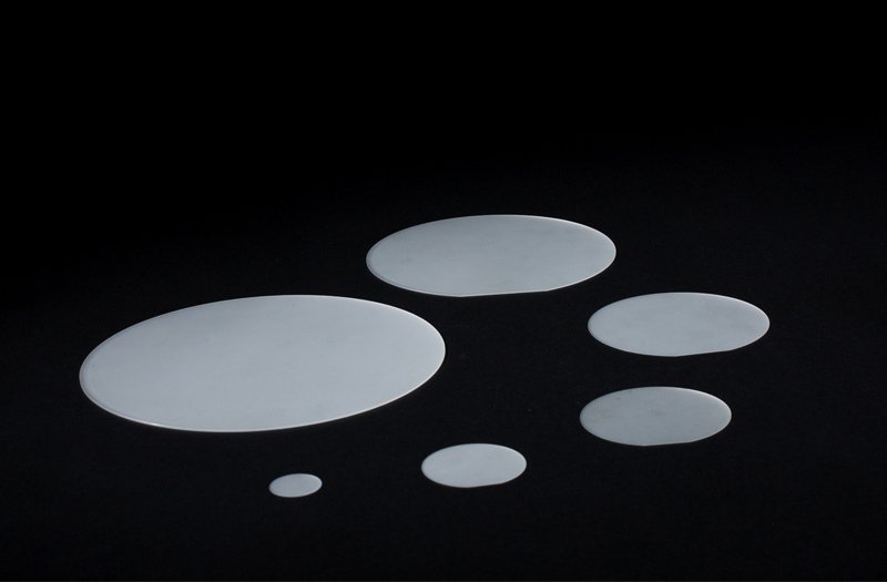
4-Inch Al₂O₃ Sapphire Wafer Product Introduction
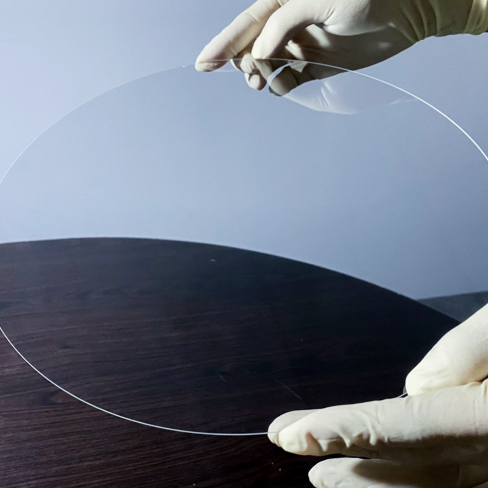
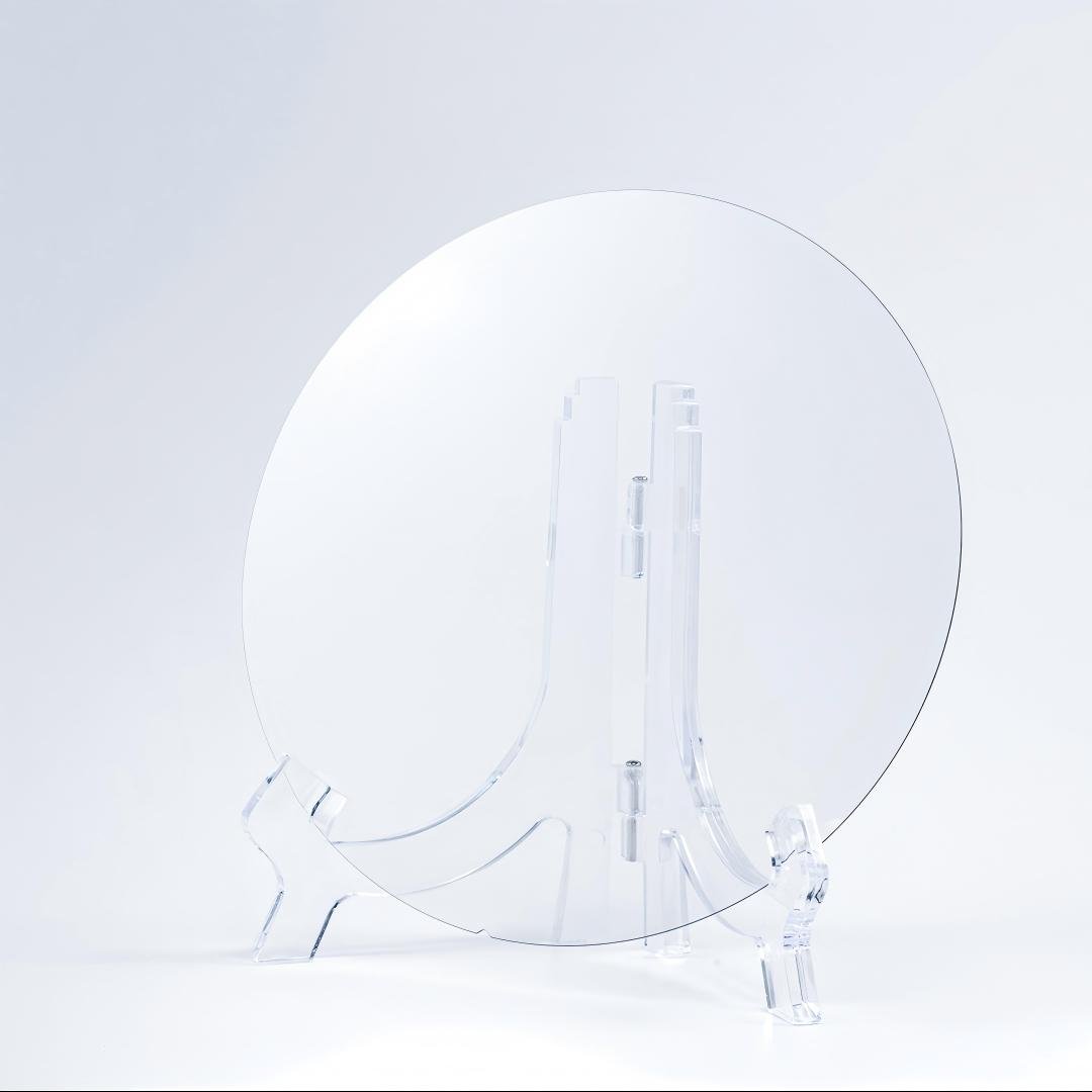
The sapphire wafer is one of the most reliable and versatile substrates for advanced technologies. As industries continue to demand high-performance materials, engineers and researchers consistently choose the 4-inch Al₂O₃ sapphire wafer. This product combines optical transparency, high mechanical strength, electrical insulation, and thermal stability into a single substrate, so you gain performance and durability simultaneously. Because sapphire belongs to the corundum family and ranks 9 on the Mohs hardness scale, the wafer provides excellent scratch resistance and chemical durability, and therefore it becomes indispensable for applications ranging from microelectronics to optoelectronics.
Why 4-Inch Sapphire Wafer Stands Out
You should consider the 4-inch sapphire wafer for several reasons. First, the size strikes a balance between research flexibility and production scalability. While smaller wafers serve laboratory experiments, and larger wafers dominate mass production, the 4-inch sapphire wafer remains the most widely adopted format for prototyping, testing, and niche high-volume runs.
Second, the sapphire wafer offers superior crystalline quality, and because it is grown from high-purity Al₂O₃ (≥99.99%), it minimizes defects during epitaxy. You gain surfaces that reduce dislocations in GaN and other III-V materials, which in turn boosts device efficiency.
Third, sapphire wafer provides excellent optical clarity across ultraviolet, visible, and infrared ranges. This feature ensures that devices like LEDs, laser diodes, and optical sensors can operate efficiently. Moreover, the wafer resists thermal shock, and it tolerates rapid heating and cooling cycles without cracking.
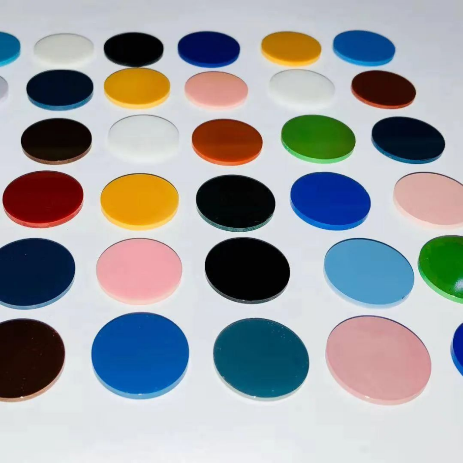
Finally, the 4-inch sapphire wafer supports versatile orientations—C-plane, A-plane, R-plane, and M-plane—so you can select the most suitable crystallographic orientation depending on your growth requirements. For example, C-plane wafers dominate GaN LED production, while R-plane and A-plane wafers serve different photonics or RF applications.
Key Features of Sapphire Wafer
High hardness and durability: Sapphire wafer resists scratching and mechanical wear, and you benefit from stable long-term device performance.
Thermal resistance: You can process devices at temperatures above 1000 °C with no warping.
Low dielectric loss: You use sapphire wafer for RFIC, microwave, and insulating layers with confidence.
Transparency from UV to IR: You ensure reliable optical transmission, and this helps in lasers, detectors, and sensors.
Surface quality: You receive epi-ready wafers with surface roughness <0.5 nm for defect-free epitaxy.
Dimensional stability: You rely on strict control of TTV, bow, and warp, so yield improves.
Because sapphire wafer integrates these properties, you gain efficiency at every stage—from wafer processing to final device assembly.
Technical Specification Table
| Parameter | Specification (Typical) |
|---|---|
| Material Purity | ≥ 99.99% Al₂O₃ single crystal |
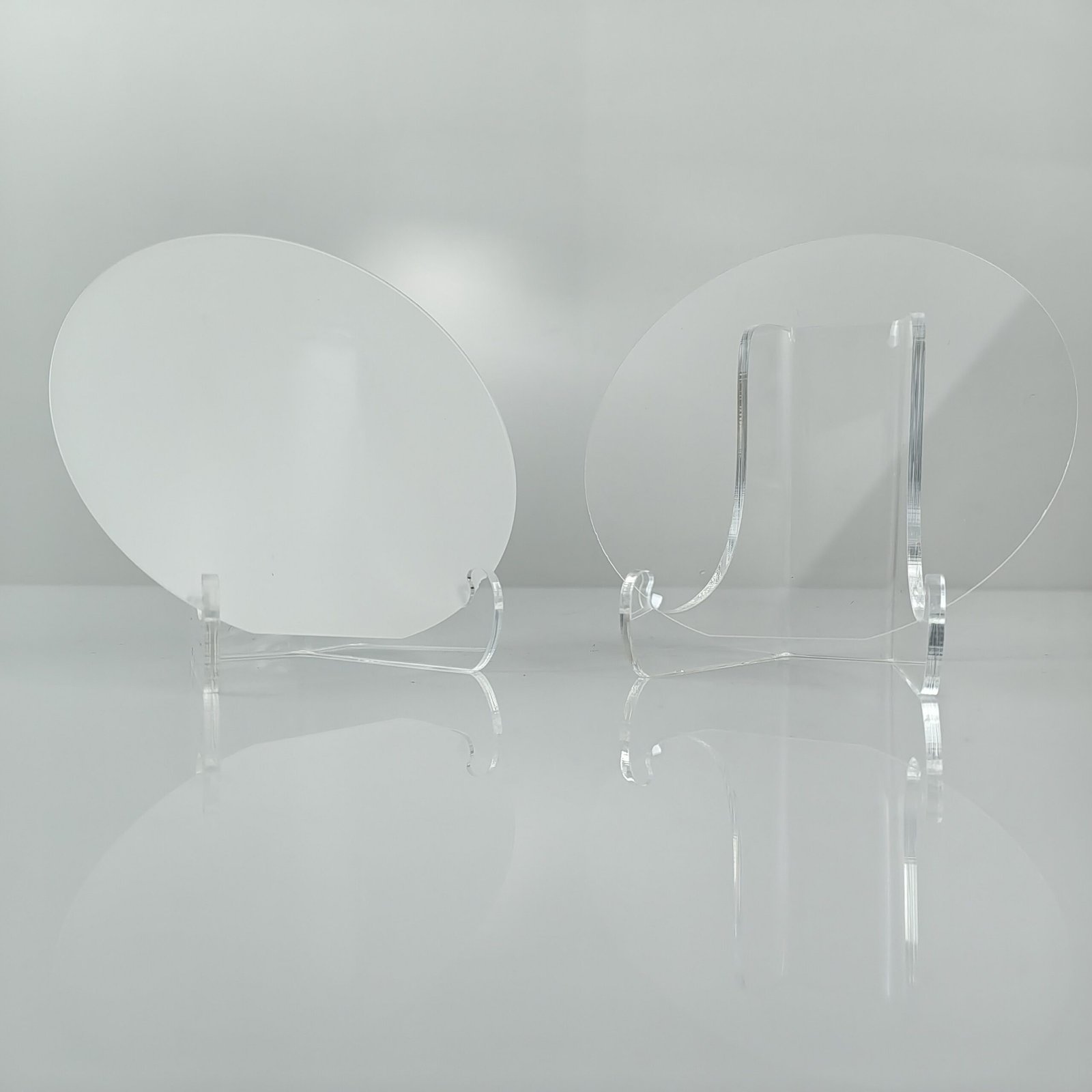
| Diameter | 100 mm ± 0.1 mm (≈ 4 inch) |
| Thickness | SSP: 650 µm ± 25 µm; DSP: 600 µm ± 25 µm |
| Orientation | C-plane (0001) standard; A, R, and M available on request |
| Surface Finish | SSP: front side epi-ready < 0.5 nm Ra; DSP: both sides polished |
| TTV / Bow / Warp | < 20 µm |
| Edge Profile | Rounded or beveled (standard SEMI specifications) |
| Thermal Expansion Coefficient | 6.66 × 10⁻⁶ /°C (‖ C-axis); 5.0 × 10⁻⁶ /°C (⟂ C-axis) |
| Thermal Conductivity | 30–42 W/(m·K) at 20–25 °C |
| Dielectric Constant | ~11.5 (‖ C-axis); ~9.3 (⟂ C-axis) |
| Dielectric Strength | ~4.8 × 10⁵ V/cm |
| Refractive Index | ~1.77 in visible spectrum |
| Optical Transmission | 200 nm – 5 µm range |
| Mohs Hardness | 9 |
Applications of Sapphire Wafer
Because sapphire wafer combines optical, electrical, and mechanical advantages, you see it applied in multiple industries:
LED Production
GaN-on-sapphire LED production dominates global lighting and display markets. You use C-plane wafers to grow GaN epitaxy with low defect density, and you achieve higher efficiency LEDs for consumer electronics, automotive lighting, and backlighting.Laser and Photonics
You rely on sapphire wafer in solid-state lasers, photodetectors, and UV optics. Because the wafer transmits across a wide spectrum, you ensure consistent performance in demanding optical systems.Semiconductors and RFIC
In RFIC and SOS technologies, sapphire wafer acts as an insulator with low dielectric loss, and you achieve faster, more reliable signal transmission.Watch and Consumer Electronics
Although thin sapphire glass protects watch faces, sapphire wafer also supports cover windows for smartphones, sensors, and cameras. Its hardness resists scratches while maintaining transparency.Research and Prototyping
Because 4-inch sapphire wafer balances cost and size, universities and labs choose it for pilot runs. It helps researchers develop next-generation semiconductor and photonic devices before scaling to larger wafers.
Manufacturing and Processing Advantages
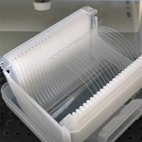
Suppliers produce sapphire wafer through advanced crystal growth methods such as the Kyropoulos (KY) or Czochralski (CZ) technique. You benefit from uniform crystalline quality, because the growth process minimizes dislocations. After crystal growth, manufacturers cut ingots into wafers, then grind, lap, and polish surfaces using diamond-based abrasives.
You receive wafers with consistent thickness, minimal TTV, and optical-grade surface finishes. You can also request custom features such as laser scribing, orientation flats, or custom bevel profiles. Because polishing processes reduce surface roughness to sub-nanometer levels, you achieve smooth surfaces ready for epitaxy without additional steps.
Choosing the Right Sapphire Wafer
When you select a sapphire wafer, you should evaluate key factors:
Orientation: C-plane for LEDs and GaN epitaxy, A-plane for optical windows, R-plane for photonics.
Polish Type: SSP if you require one epi-ready side; DSP if both sides must remain flat and clean.
Thickness: Choose based on your process tolerance and mechanical strength needs.
Customization: Request patterned wafers, drilled vias, or laser marking depending on your design.
By aligning wafer specifications with your application, you ensure high yield and device reliability.
Advantages Over Alternative Substrates
Although SiC, Si, and GaAs compete as substrates, sapphire wafer maintains unique benefits. Unlike Si, sapphire withstands extreme heat and does not melt in standard processing ranges. Compared to GaAs, sapphire is harder, more chemically stable, and more affordable for large-volume LED production. And while SiC delivers conductivity advantages, sapphire remains cost-effective and optically transparent, so it dominates optoelectronics.
Q&A: All About Sapphire Wafer
Q: Why do engineers prefer sapphire wafer for GaN LEDs?
A: You gain low lattice mismatch, good transparency, and cost efficiency, so sapphire wafer remains the leading substrate for LED production.
Q: Can sapphire wafer replace silicon wafer?
A: You cannot fully replace silicon wafer, because silicon suits CMOS and logic devices; however, sapphire wafer outperforms silicon in optoelectronics, high-frequency, and high-temperature fields.
Q: How do I decide between SSP and DSP sapphire wafer?
A: You select SSP when only one side requires epitaxy, and you choose DSP when both sides must remain highly polished for optical or MEMS applications.
Q: What sizes are available beyond 4-inch sapphire wafer?
A: Suppliers offer sapphire wafer in 2-inch, 6-inch, 8-inch, and even 12-inch, but 4-inch remains most versatile for cost-effective development.
Q: How does sapphire wafer compare to quartz?
A: While quartz provides transparency, sapphire wafer delivers superior hardness, thermal resistance, and dielectric strength, so it supports more demanding applications.
Q: Is sapphire wafer cost-effective?
A: Yes. You invest more initially than with glass or quartz, but you save long-term due to lower defect rates, higher yields, and longer device lifetimes.
