


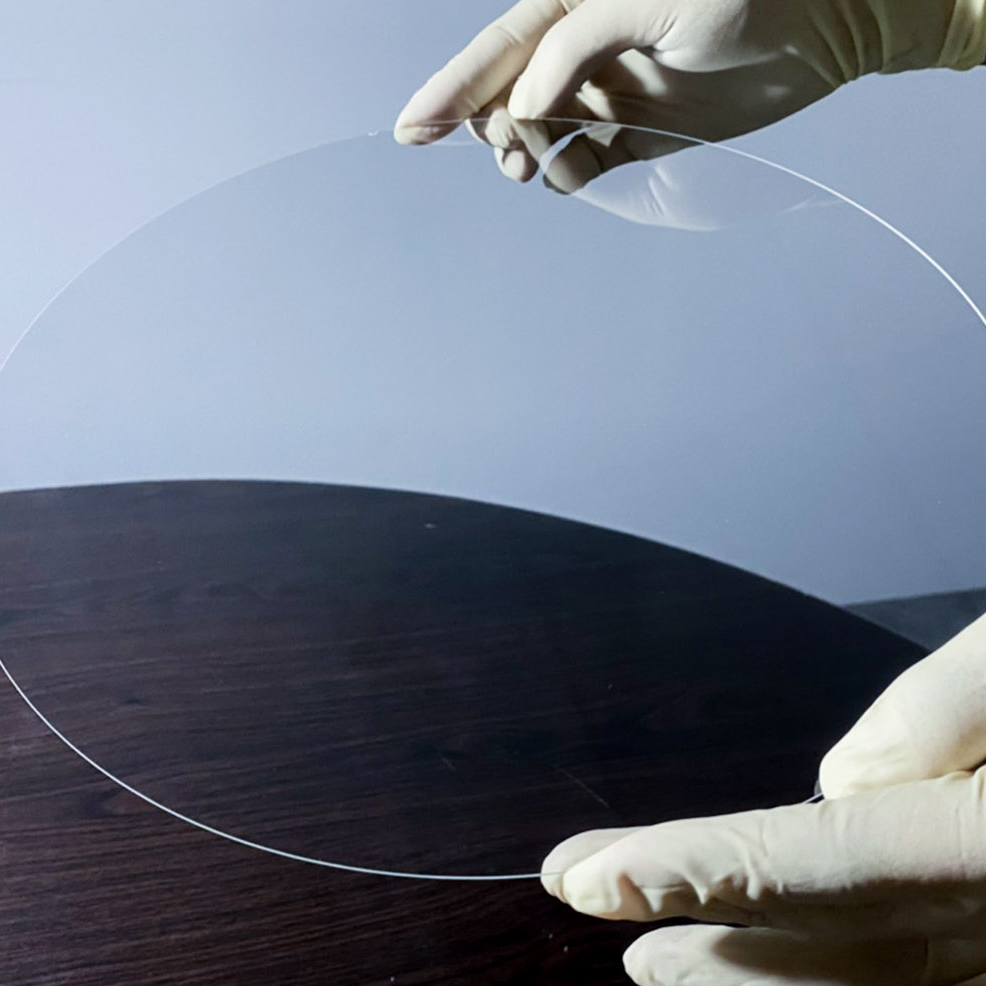
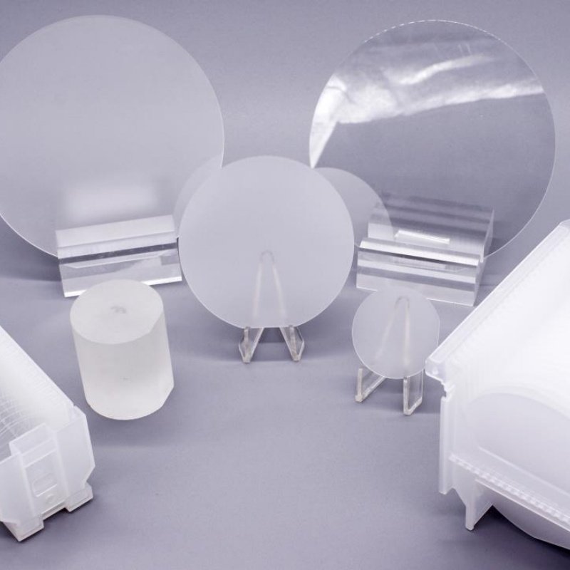
Product Introduction of sapphire wafer
A sapphire wafer is a wafer-grade material made from single-crystal Al₂O₃. It features excellent optical transmittance from deep UV to infrared. It has an ultra-high hardness of Mohs 9 and exceptional chemical stability.
These qualities make it a key material in advanced manufacturing worldwide. Compared with conventional silicon wafers, sapphire wafers withstand extreme high temperatures.
They also maintain stability under acidic, alkaline, and mechanical wear conditions. They are widely used in LED chips, laser windows, infrared detectors, sapphire optical lenses, and sensors. In semiconductor epitaxy and optoelectronic device production, a sapphire wafer provides a stable crystal lattice.
This enables high-quality gallium nitride (GaN) epitaxial growth. Such growth improves device performance and extends service life. For these reasons, sapphire wafers are regarded as fundamental materials for energy-efficient lighting. They are also essential for optical communication devices. We also provide the SiC wafer.
Manufacturing Principle of sapphire wafer
The production of sapphire wafers begins with melting high-purity aluminum oxide at extreme temperatures, typically using the Kyropoulos method, Czochralski method, or Heat Exchange Method (HEM) to grow single-crystal sapphire.
Kyropolos for sapphire
In the Kyropolos method, sapphire is extracted from a melt by crystallization. The process involves melting high-purity aluminium oxide (Al₂O₃) and then slowly cooling it to crystallize the molten material. This process forms large sapphire crystals. Manufacturers cut these crystals into slices and polish them to produce sapphire wafers. The Kyropoulos method produces sapphire wafers with high purity and crystal quality. Its uniform structure and high transparency make it ideal for optoelectronics and LED applications.
HEM (Heat Exchanger Method) for sapphire
HEM (Heat Exchanger Method):
The HEM method for producing sapphire wafers crystallizes sapphire from a liquid aluminium oxide mixture.
A heating medium transfers heat away to cool the mixture. This cooling forms sapphire crystals at the interface between the melt and the cooling medium. Compared to the Kyropoulos method, the HEM method crystallizes sapphire faster and increases production rates.
However, it can produce wafers with lower crystal quality and less uniformity. During crystal growth, engineers precisely control temperature gradients, rotation speeds, and cooling rates.
These controls reduce internal stress and crystal lattice defects. They also yield high-purity, high-transparency sapphire crystals.
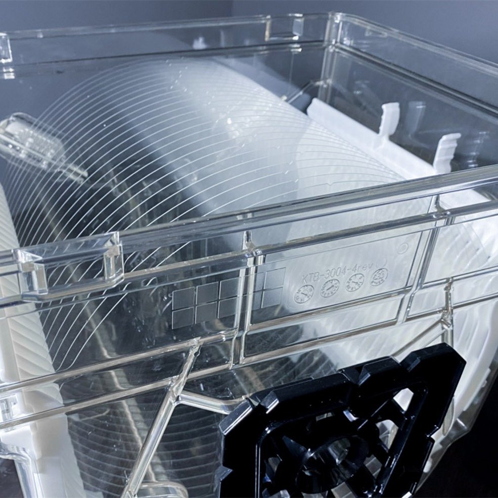
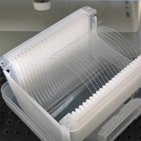
Manufacturers orient the sapphire boules (C-plane, A-plane, R-plane, etc.), slice them, lap them, and fine-grind them. They then perform chemical mechanical polishing (CMP) to achieve sub-nanometer surface roughness.
This advanced manufacturing process ensures optical uniformity in sapphire wafers. It also delivers excellent adhesion and stability during epitaxial deposition and chip fabrication.
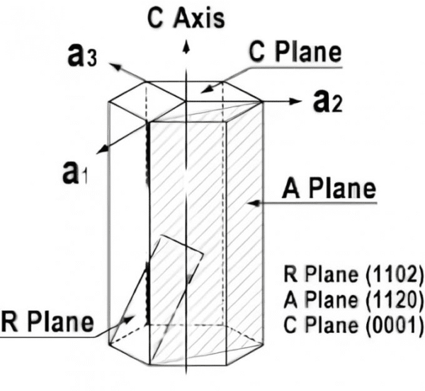
C-A-R-M of sapphire
C-A-R-M stands for the Miller indices of the crystal axes in the hexagonal structure of sapphire. The letters correspond to the axis directions [1-100], [11-20], [1-102] and [1-101]. The “C-A-R-M plane” refers to a specific crystal plane within the sapphire crystal, which is defined by the arrangement of the atoms along these axes.
The crystal plane influences properties of the sapphire wafer, such as electrical, optical, or mechanical characteristics.
These effects make it important for certain applications in the semiconductor industry, optoelectronics, and other fields.
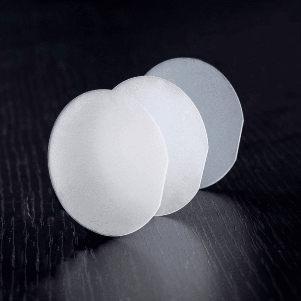
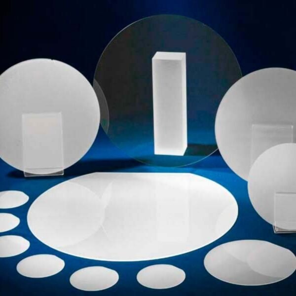
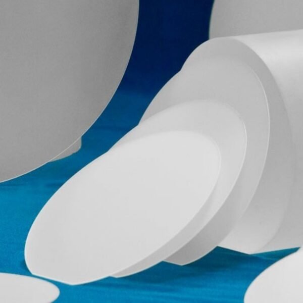
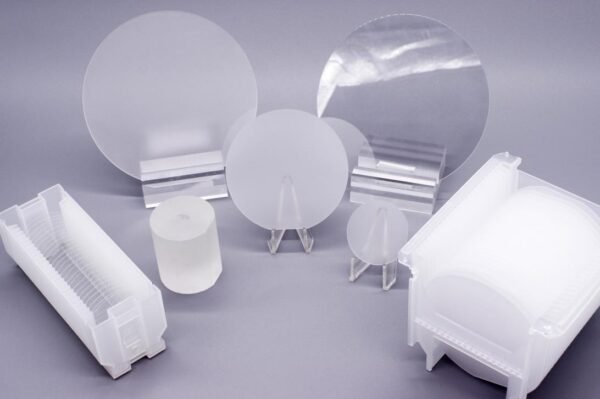
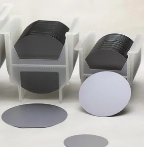
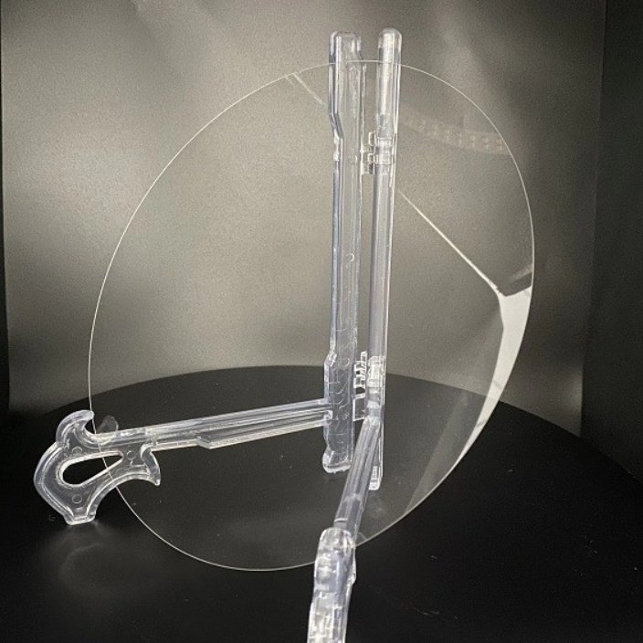
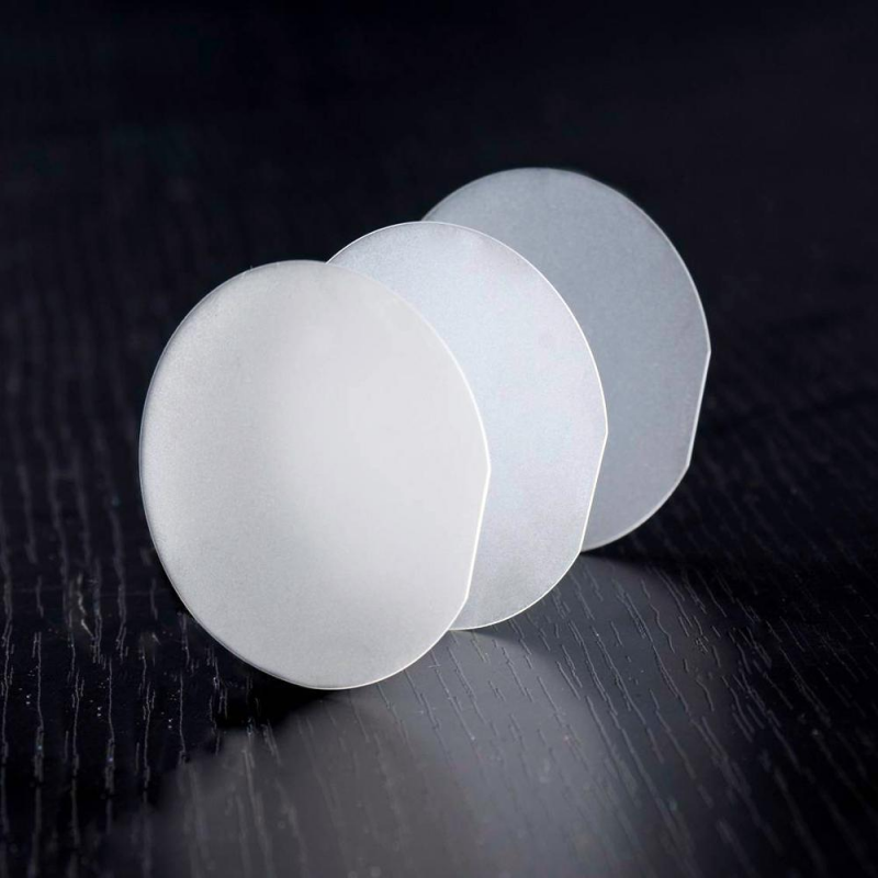
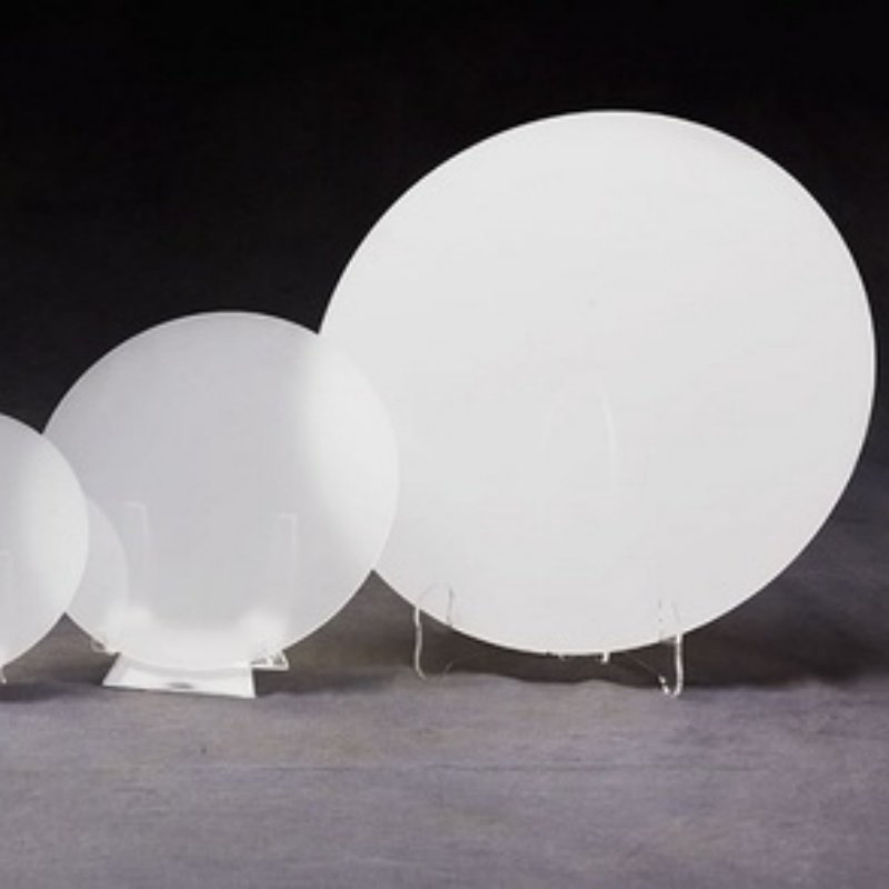
Common Categories of sapphire wafer
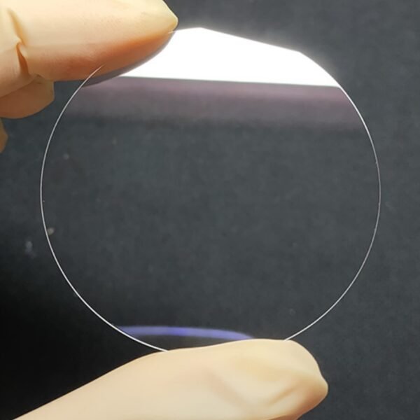
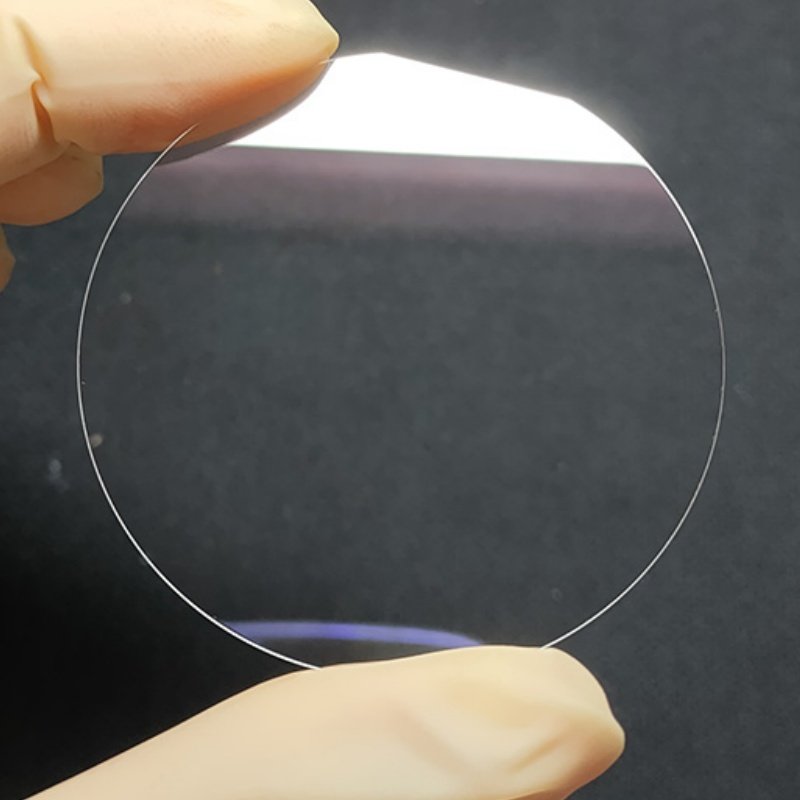
Single-Side Polished Sapphire Wafer
Optical polishing on one side, mechanically lapped on the other; cost-effective for optical testing and certain research uses.
Double-Side Polished Sapphire Wafer
Nanometer-level polishing on both sides, minimal surface defects; ideal for LED epitaxy, lasers, and precision optical devices.
C-Plane Sapphire Wafer (0001 Orientation)
The most common orientation for GaN epitaxial growth; offers high lattice match and low dislocation density.
A-Plane Sapphire Wafer (11-20 Orientation)
Suitable for specific laser and optical coating applications.
R-Plane Sapphire Wafer (1-102 Orientation)
Commonly used in infrared windows, polarizers, and other optical components.
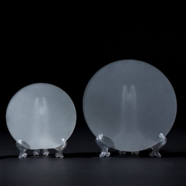
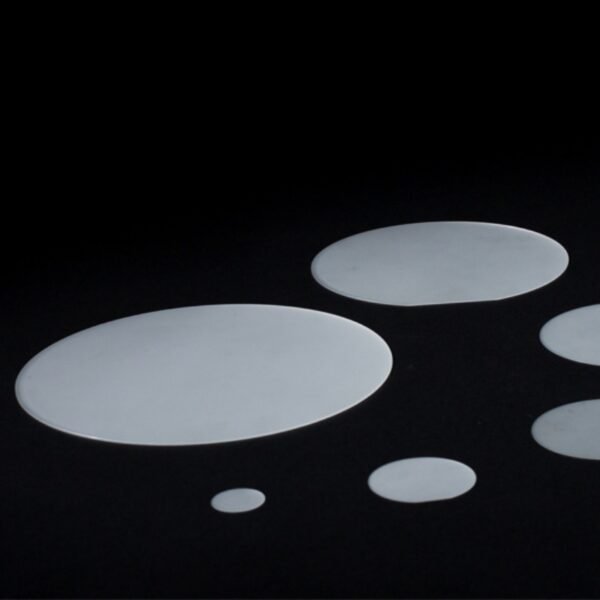
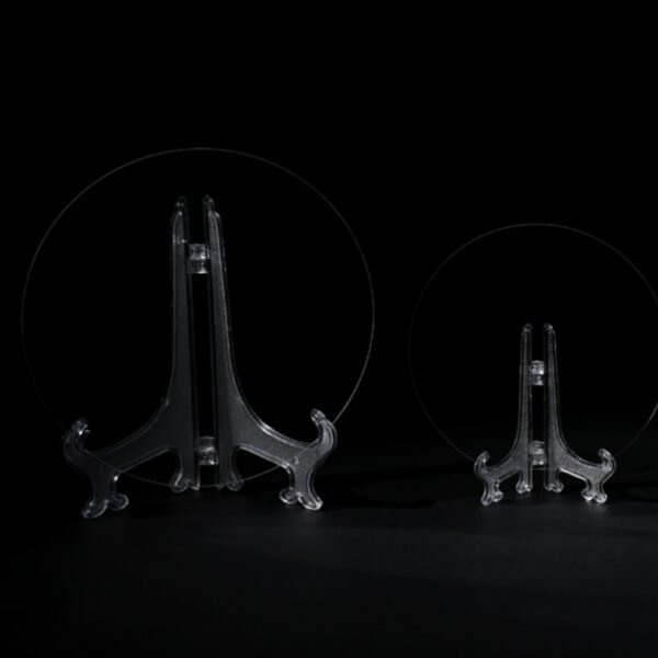
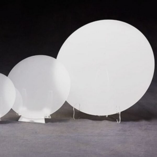
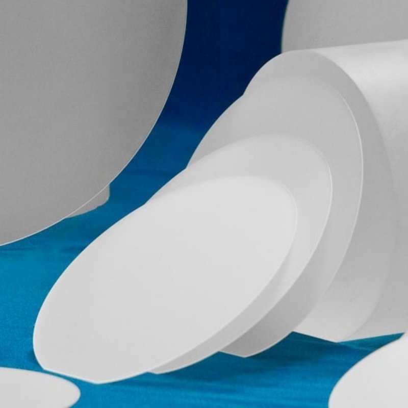
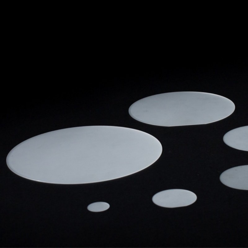
Custom Size & Thickness Sapphire Wafer
Available in diameters from 2-inch to 8-inch, thicknesses from 0.3 mm to 2 mm, with customizable tolerances and orientations.
Specification of sapphire wafer
| Item | Standard Specification | ||||
|---|---|---|---|---|---|
| Diameter | 2 inch | 4 inch | 6 inch | 8 inch | 12 inch |
| Material | Artificial sapphire( Al2O3 ≥ 99.99%) | ||||
| Thickness | 430±15μm | 650±15μm | 1300±20μm | 1300±20μm | 3000±20μm |
| Surface orientation | c-plane(0001) | ||||
| OF length | 16±1mm | 30±1mm | 47.5±2.5mm | 47.5±2.5mm | *negotiable |
| OF orientation | a-plane 0±0.3° | ||||
| TTV * | ≦10μm | ≦10μm | ≦15μm | ≦15μm | *negotiable |
| BOW * | -10 ~ 0μm | -15 ~ 0μm | -20 ~ 0μm | -25 ~ 0μm | *negotiable |
| Warp * | ≦15μm | ≦20μm | ≦25μm | ≦30μm | *negotiable |
| Front side finishing | Epi-ready (Ra<0.3nm) | ||||
| Back side finishing | Lapping (Ra 0.6 – 1.2μm) | ||||
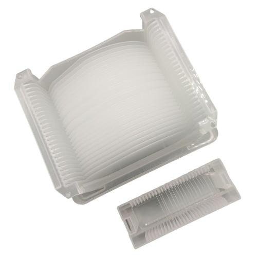
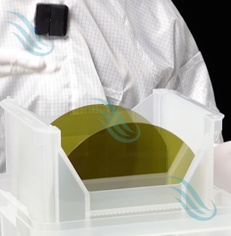
| Packaging | Vacuum packaging in clean room | ||||
| Prime grade | High quality cleaning : particle size ≧ 0.3um), ≦ 0.18pcs/cm2, metal contamination ≦ 2E10/cm2 | ||||
| Remarks | Customizable specifications: a/ r/ m-plane orientation, off-angle, shape, double side polishing | ||||
Applications of sapphire wafer
Sapphire wafers play an irreplaceable role in various advanced industries:
LED & Laser Manufacturing: As a substrate for GaN epitaxial growth, sapphire wafers provide a flat, stable lattice structure that enhances luminous efficiency and lifespan.
Optical & Infrared Windows: High transmittance and superior scratch resistance make sapphire wafers ideal for laser windows, detector covers, and infrared camera lenses.
Semiconductors & RF Devices: In high-frequency, high-power RFICs and microwave integrated circuits, sapphire wafers help minimize parasitic effects and improve signal transmission.
High-Temperature & Corrosive Environments: Sapphire wafers remain stable at up to 2000°C and in strong acids or alkalis, making them ideal for sensors and protective components in extreme industrial environments.

Product FAQ of sapphire wafer
Q1: Can the diameter and thickness of sapphire wafers be customized?
A1: Yes. We offer standard diameters from 2-inch to 8-inch and thicknesses from 0.3 mm to 2 mm, with precise tolerances and orientations customized to meet your process requirements.
Q2: Are sapphire wafers more expensive than silicon wafers?
A2: Yes. Long production cycles and high processing difficulty make sapphire wafers more costly than silicon wafers. In LEDs, high-power lasers, and optical windows, sapphire wafers provide unmatched high-temperature resistance, wear resistance, and optical performance—delivering superior overall value.
Q3: How is the quality of sapphire wafers ensured?
A3: We use strict crystal growth control, fully automated slicing and polishing equipment, and advanced inspection tools such as interferometers and X-ray diffraction to guarantee wafer flatness, orientation accuracy, and surface quality.
Wikipedia link:https://en.wikipedia.org/wiki/Sapphire
Related Product
