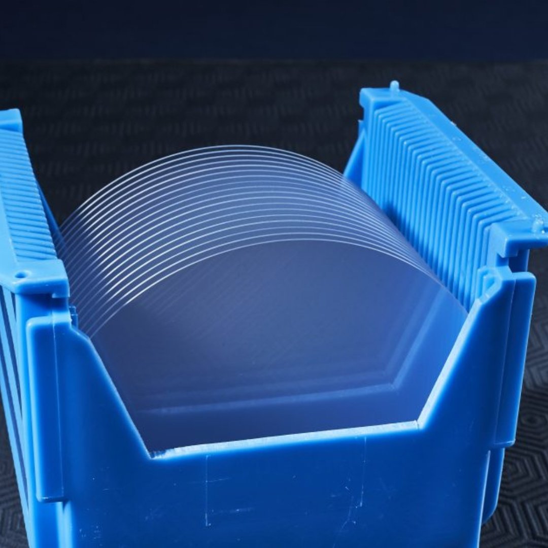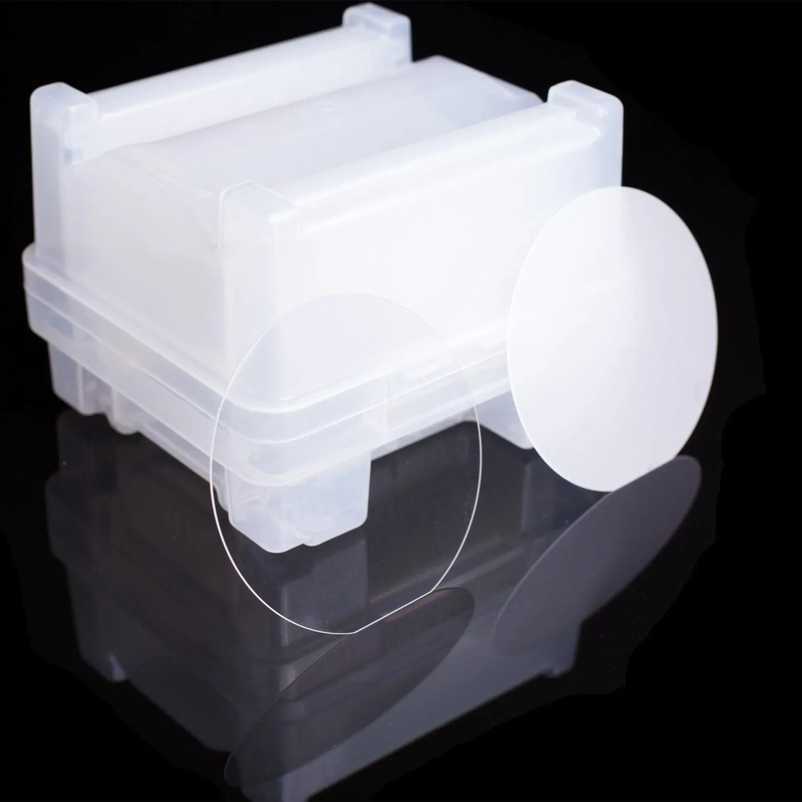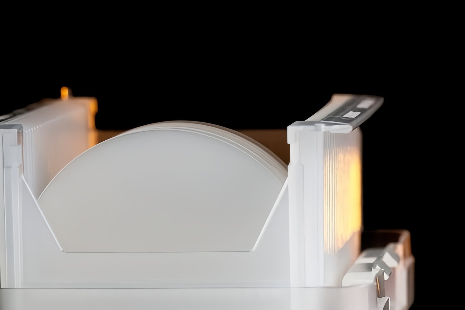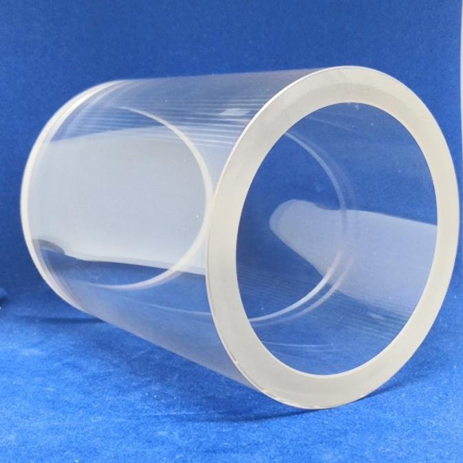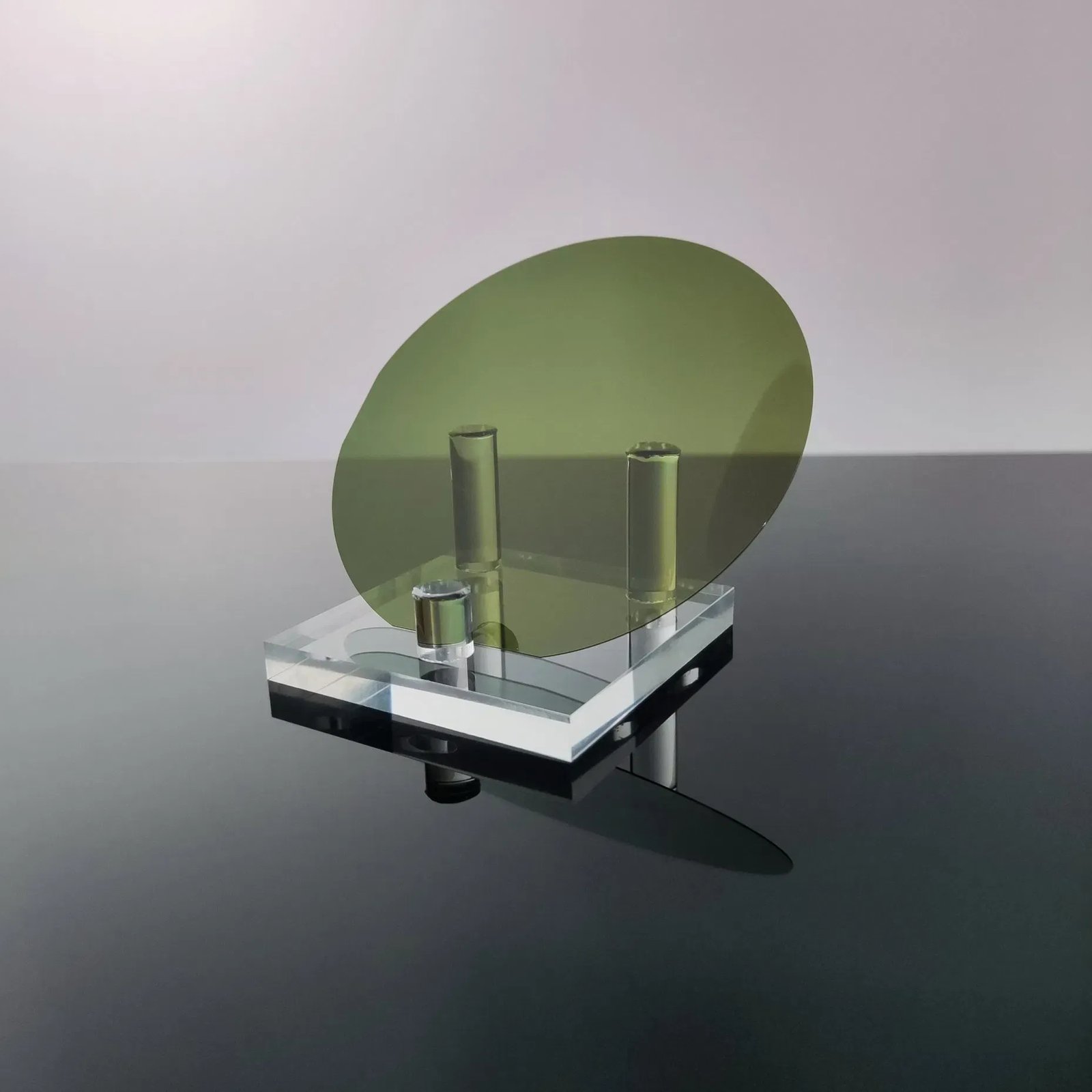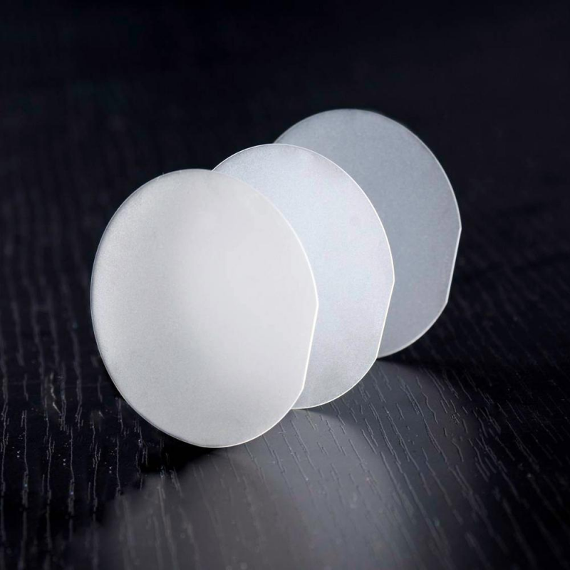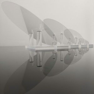

2-Inch Al₂O₃ Sapphire Wafer / Substrate – Precision Material for Advanced Applications
The sapphire wafer represents one of the most trusted and versatile substrates in modern technology. When you choose a 2-inch Al₂O₃ sapphire wafer, you gain access to a material that combines superior hardness, high thermal resistance, optical transparency, and excellent dielectric properties. Because of these characteristics, the 2-inch sapphire wafer is widely adopted in research institutions, universities, pilot production lines, and specialty device manufacturers.
You not only benefit from its cost efficiency compared with larger diameters, but you also maintain consistent crystalline quality. Moreover, the wafer provides mechanical strength and chemical stability, so you use it in harsh environments without sacrificing performance. With this substrate, you drive progress in semiconductors, photonics, optoelectronics, and microwave communications.
Why the 2-Inch Sapphire Wafer Stands Out
The 2-inch sapphire wafer occupies a unique position in the market. While larger wafers (4-inch, 6-inch, or 8-inch) dominate high-volume commercial production, the 2-inch wafer supports early-stage R&D, small-scale prototyping, and advanced testing. You often prefer this format because it balances manageable cost with robust performance.
You gain substrates that minimize lattice mismatch during GaN epitaxy, and you ensure that LEDs, laser diodes, and UV detectors achieve higher efficiency. Additionally, sapphire’s Mohs hardness of 9 guarantees surface durability, and this feature extends device longevity. Since the wafer transmits light from the UV region to the IR spectrum, you also expand its use in optical components. Furthermore, its electrical insulation and low dielectric loss make it highly suitable for RF and SOS (silicon-on-sapphire) devices.
Key Benefits of Sapphire Wafer
Superior Purity: You use Al₂O₃ material with ≥99.99% purity, so you reduce impurity-related defects.
Dimensional Precision: You rely on thickness uniformity and minimal TTV to maintain fabrication accuracy.
Surface Quality: You obtain epi-ready polish with sub-nanometer roughness, which ensures smooth epitaxial growth.
Thermal Reliability: You process devices at >1000 °C confidently, as sapphire wafer resists warping and cracking.
Optical Transparency: You benefit from transmission across 200 nm–5 µm, which covers UV, visible, and IR applications.
Mechanical Strength: You exploit hardness and chemical inertness, which protect devices in extreme environments.

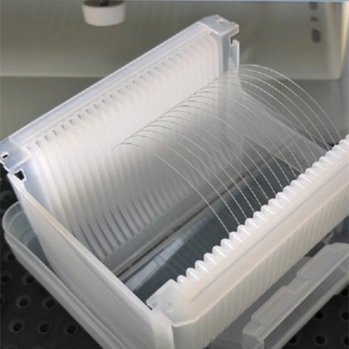
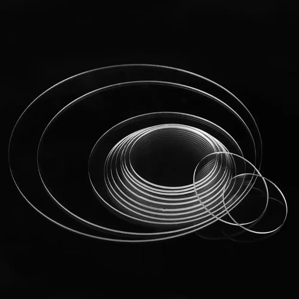
Technical Specifications of 2-Inch Sapphire Wafer
| Parameter | Specification (Typical) |
|---|---|
| Material Purity | ≥ 99.99% Al₂O₃ single crystal |
| Diameter | 50.8 mm ± 0.1 mm (≈ 2 inch) |
| Thickness | 430 µm ± 15 µm (SSP or DSP) |
| Orientation | C-Plane (0001) standard; A-, R-, M-planes available |
| Surface Finish | SSP: front side Ra < 0.3 nm; DSP: both sides Ra < 0.3 nm |
| TTV / Bow / Warp | < 10 µm |
| Primary Flat & Length | A-plane orientation, flat length ~16 mm ± 1 mm |
| Edge Profile | Standard SEMI chamfer or custom bevel |
| Thermal Expansion Coefficient | ∥ C-axis: 6.66 × 10⁻⁶ /°C; ⟂ C-axis: 5.0 × 10⁻⁶ /°C |
| Thermal Conductivity | 30–42 W/(m·K) at ~20–25 °C |
| Dielectric Constant | ~11.5 (∥ C-axis); ~9.3 (⟂ C-axis) |
| Dielectric Strength | ~4.8 × 10⁵ V/cm |
| Refractive Index | ~1.77 in visible spectrum |
| Optical Transmission | 200 nm – 5 µm |
| Mohs Hardness | 9 |
Applications of 2-Inch Sapphire Wafer
1. LED and Optoelectronics
You rely on 2-inch sapphire wafer for GaN epitaxy, and you ensure high-efficiency blue and UV LEDs. Because sapphire’s transparency enhances light extraction, you boost LED output while maintaining cost control.
2. Lasers and Photonics
You use sapphire wafer in solid-state lasers, optical filters, and photodetectors. Its wide spectral transmission and hardness allow you to design durable and efficient photonic devices.
3. RF and SOS Devices
You select sapphire wafer for RFIC and SOS structures because its dielectric properties reduce signal loss. With low dielectric constant and strong electrical insulation, you support high-frequency circuits reliably.
4. MEMS and Sensors
You integrate sapphire wafer into MEMS pressure sensors, micro-fluidic chips, and bio-optical devices. Its mechanical resilience and transparency help you create precision instruments.
5. Research and Prototyping
You choose 2-inch sapphire wafer in labs because it reduces costs yet provides full-scale performance. Researchers test new device architectures before moving to larger wafers for industrial scale-up.
Production and Processing
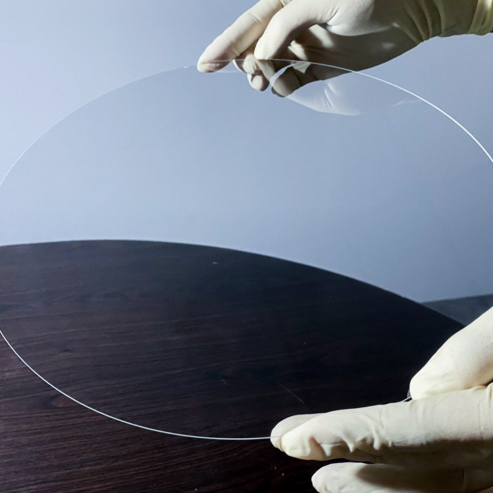
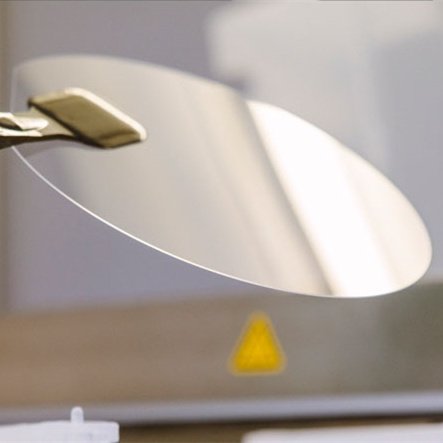
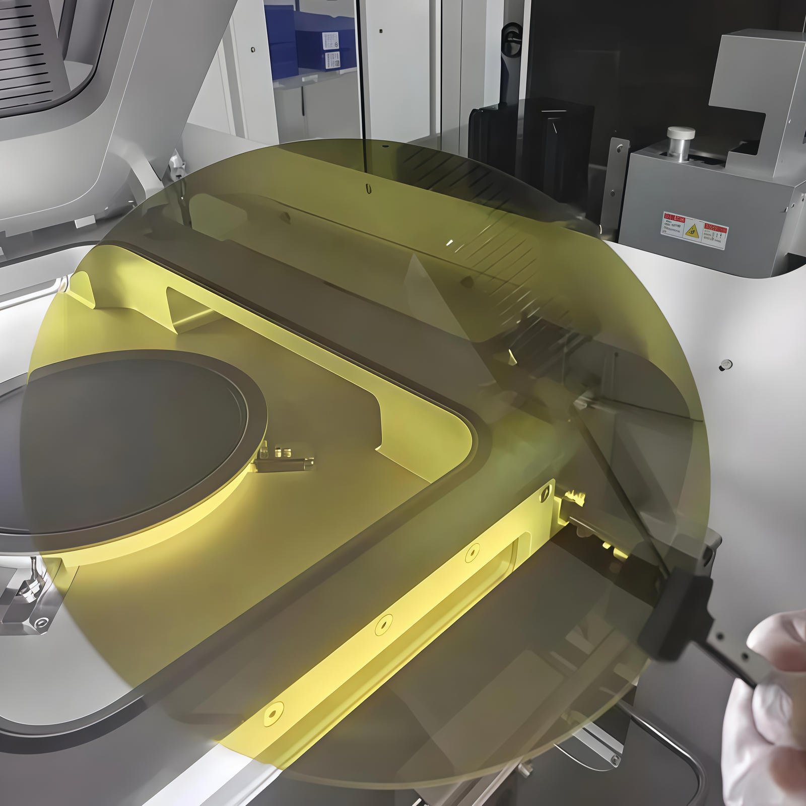
Manufacturers grow sapphire crystals through methods such as Kyropoulos (KY) or Czochralski (CZ). You benefit from uniform crystal structure with minimal dislocations. After growth, technicians slice ingots into wafers, grind and lap them to target thickness, and polish surfaces with diamond abrasives. Because the polishing process achieves Ra < 0.3 nm, you obtain defect-free epi-ready surfaces.
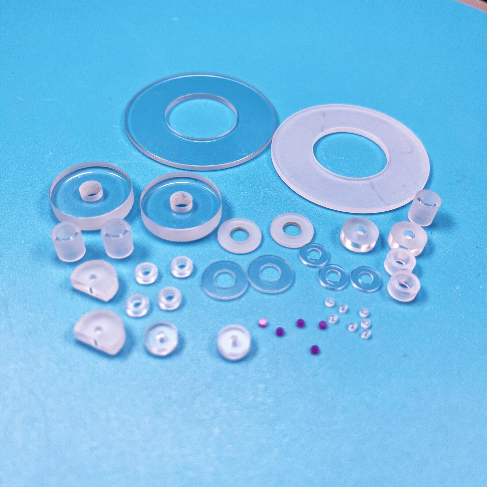
You can also request customization: orientation flats, laser scribing, drilled vias, or patterned wafers. These options allow you to adapt sapphire wafer to unique project needs. You gain flexibility while preserving quality.
Why Choose Sapphire Wafer Over Alternatives
You may ask why not silicon or SiC wafers. Silicon works well for logic devices but fails at high temperatures and lacks optical transparency. SiC offers conductivity, yet sapphire wafer remains more cost-effective for LEDs and optical applications. Glass provides transparency, yet it lacks hardness and thermal resilience. Therefore, sapphire wafer stands out because it uniquely combines mechanical hardness, optical clarity, and electrical insulation.
Final Remarks
By choosing the 2-inch sapphire wafer, you secure a material that balances affordability and performance. You achieve reliable epitaxy, durable optical performance, and stable dielectric properties. Moreover, you benefit from precise dimensions and polished surfaces that raise production yield. When your project demands reliability, sapphire wafer delivers results consistently.
Q&A: About Sapphire Wafer
Q: Why do researchers use 2-inch sapphire wafer instead of larger sizes?
A: You gain lower costs, easier handling, and the same crystal quality. That makes 2-inch sapphire wafer ideal for research and pilot projects.
Q: Which applications require C-plane sapphire wafer?
A: You use C-plane wafers for GaN-based LEDs, UV lasers, and optoelectronic devices because the lattice orientation supports efficient epitaxy.
Q: How does polishing type affect sapphire wafer?
A: You choose SSP when you need one epi-ready side. You pick DSP when both sides require high polish for optical or MEMS applications.
Q: Can sapphire wafer survive extreme environments?
A: Yes. You rely on its hardness, chemical resistance, and thermal stability for aerospace, defense, and high-power electronics.
Q: Is sapphire wafer more cost-effective than SiC?
A: In optoelectronics and LED production, sapphire wafer costs less and offers sufficient performance. While SiC suits power electronics, sapphire dominates LEDs and optics.