
Sapphire Wafer DSP and SSP – R-Orientation Substrates for Advanced Applications
Introduction
The rapid growth of semiconductor and optoelectronic industries demands substrates with unique orientations for specific applications. While C-plane sapphire wafers dominate LED manufacturing, other orientations such as R-plane (1-102) provide special advantages for certain optical and epitaxial processes. Therefore, engineers and researchers often select sapphire wafer in R-orientation to explore alternative device designs.
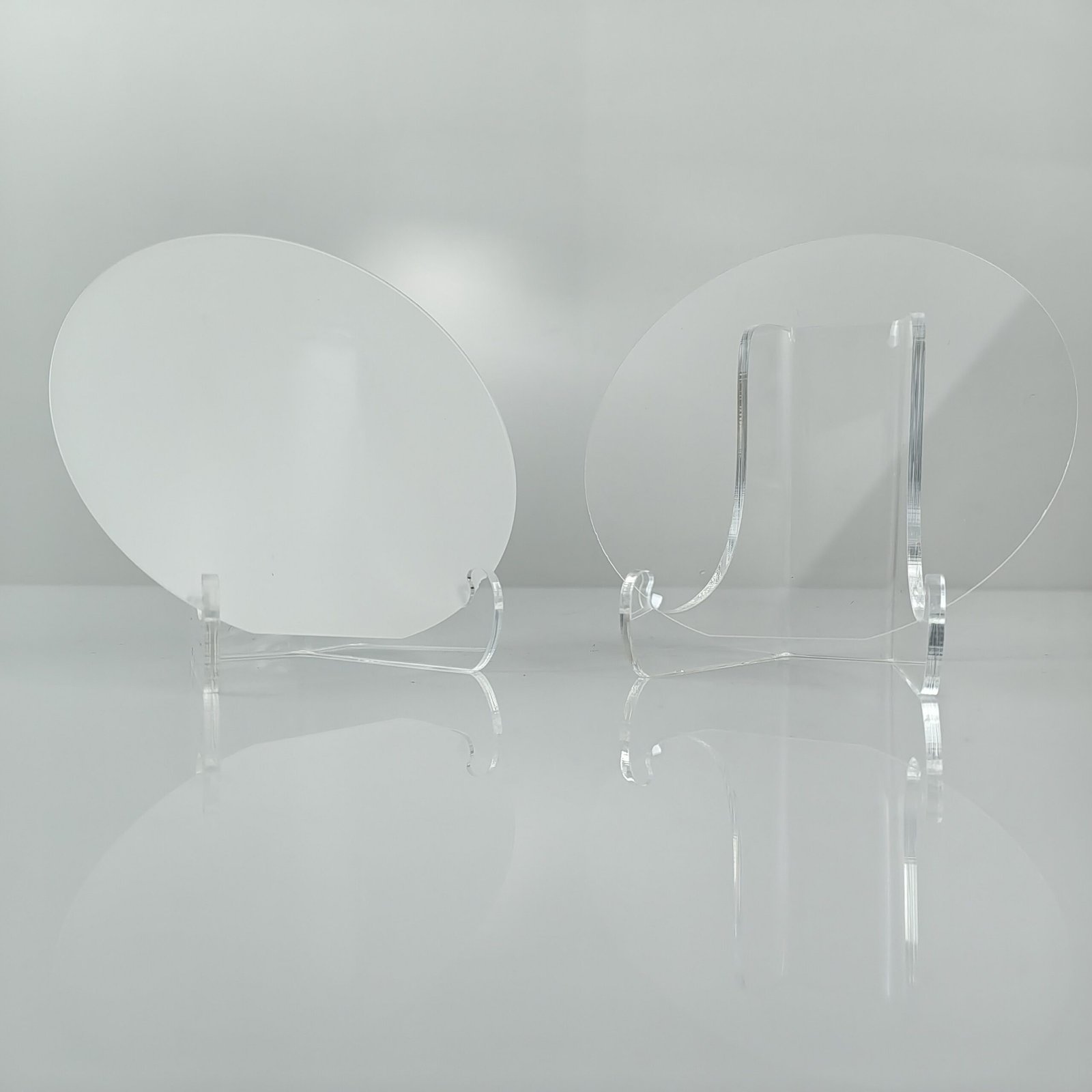
In addition, DSP (Double Side Polished) and SSP (Single Side Polished) surface finishes give customers flexibility. DSP wafers provide smooth surfaces on both sides for advanced processing, while SSP wafers deliver one epi-ready surface at a more cost-effective level. With these options, our R-orientation sapphire wafer products serve both mass production and laboratory research.
Product Overview
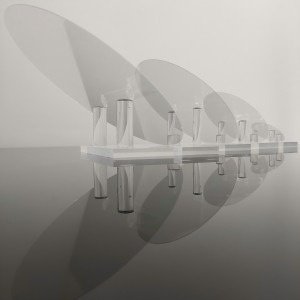
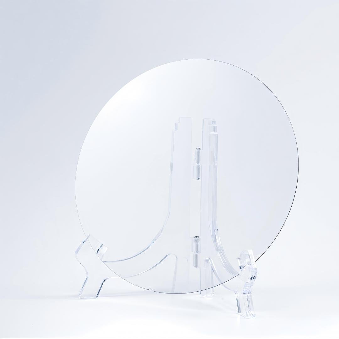
We supply high-purity sapphire wafer R-orientation (1-102) with both DSP and SSP finishing. The wafers follow strict standards for flatness, surface roughness, and contamination control. Because of excellent mechanical strength, chemical resistance, and thermal stability, these wafers support high-performance epitaxy and optical applications.
R-plane wafers align differently compared to C-plane wafers, which makes them suitable for specific epitaxial systems such as GaN or ZnO growth. Moreover, R-plane orientation offers advantages in birefringence and optical anisotropy, which expands application possibilities.
Technical Specifications
The following table presents typical parameters for sapphire wafer DSP and SSP, R-orientation:
| Item | Specification |
|---|---|
| Material | Artificial sapphire (Al₂O₃ ≥ 99.99%) |
| Orientation | R-plane (1-102) |
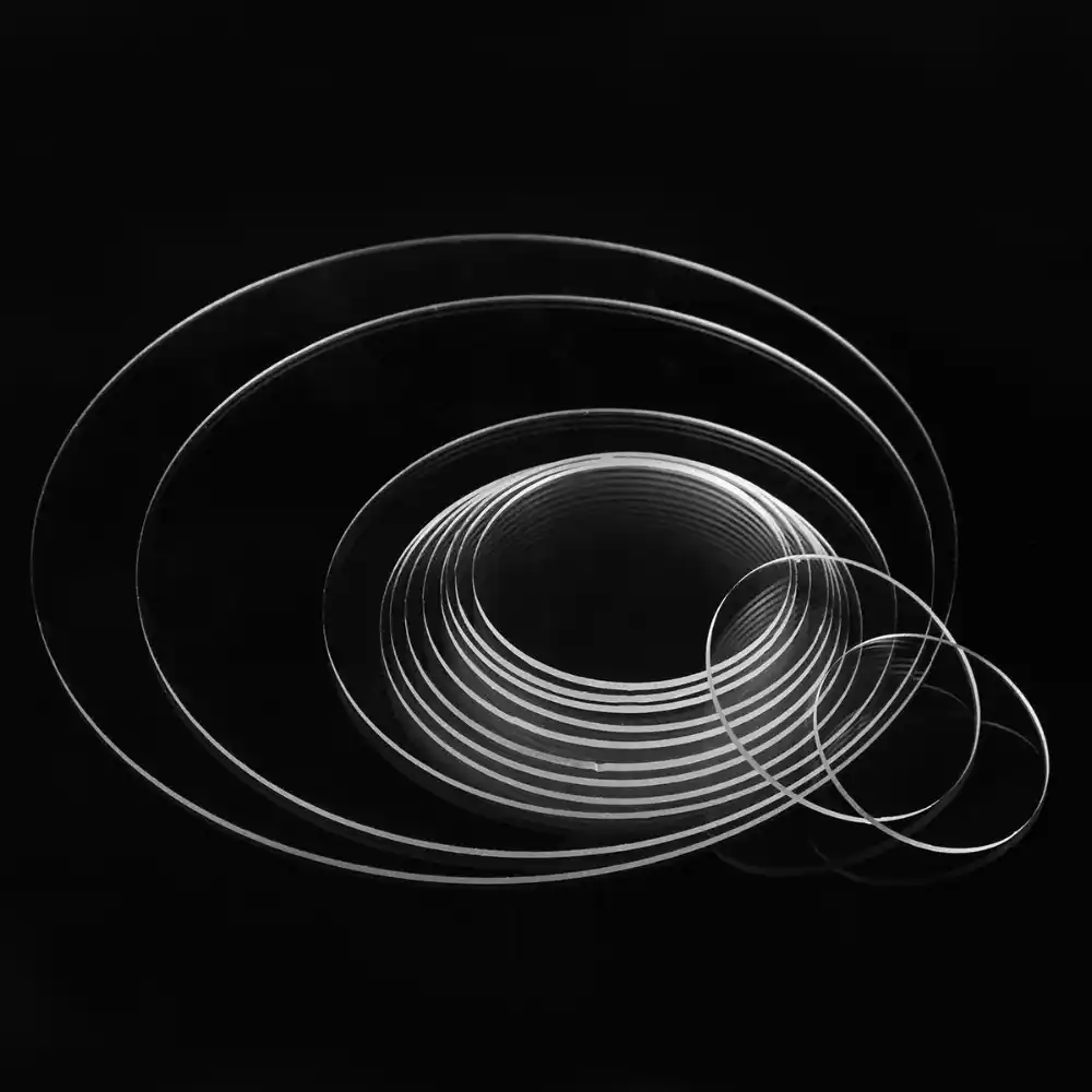
| Diameter Options | 2 inch, 4 inch, 6 inch, 8 inch, 12 inch |
| Thickness | 430 μm (2 inch), 650 μm (4 inch), 1300 μm (6–8 inch), 3000 μm (12 inch) |
| Front Side (DSP/SSP) | DSP: Double-side polished (Ra < 0.3 nm) / SSP: Single-side polished (Ra < 0.3 nm epi-ready) |
| Back Side (DSP/SSP) | DSP: Polished / SSP: Lapped (Ra 0.6 – 1.2 μm) |
| TTV | ≤ 10 μm (2–4 inch), ≤ 15 μm (6–8 inch), negotiable for 12 inch |
| BOW | -10 ~ -25 μm depending on wafer size |
| Warp | ≤ 15 – 30 μm depending on wafer size |
| OF Orientation | a-plane 0 ± 0.3° |
| OF Length | 16 mm (2 inch), 30 mm (4 inch), 47.5 mm (6–8 inch), negotiable for 12 inch |
| Surface Quality | Prime Grade: Particles ≥ 0.3 μm ≤ 0.18 pcs/cm², metal contamination ≤ 2E10/cm² |
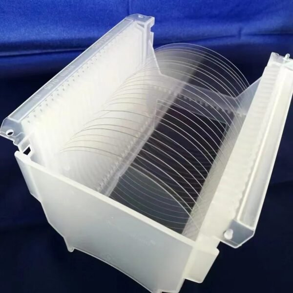
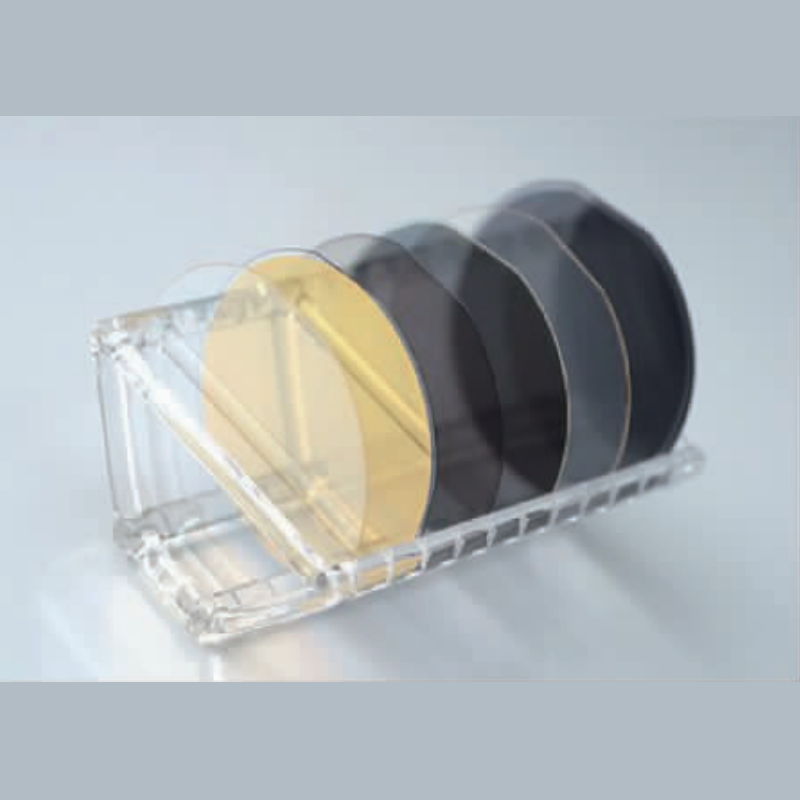
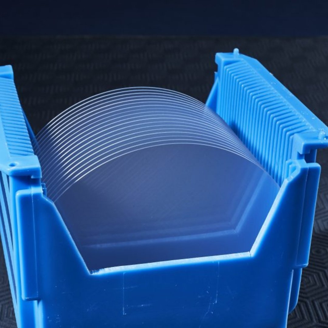
| Packaging | Vacuum packaging in cleanroom, cassette or single container |
DSP vs SSP Comparison
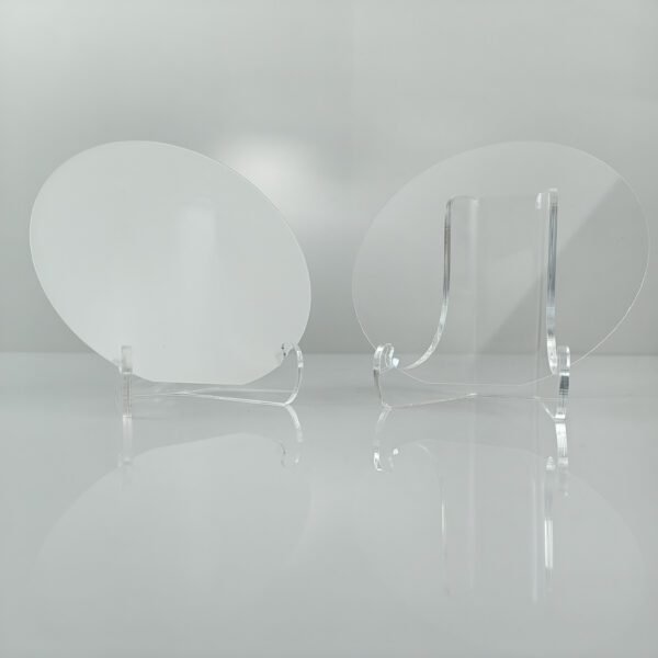
DSP Sapphire Wafer (R-orientation)
Both surfaces polished with Ra < 0.3 nm.
Supports double-sided epitaxy and advanced lithography.
Ensures optical clarity and mechanical stability.
Suitable for high-end research, optoelectronics, and specialized devices.
SSP Sapphire Wafer (R-orientation)
Front side polished to Ra < 0.3 nm.
Back side lapped with Ra 0.6 – 1.2 μm.
Offers cost-effective performance for epitaxy and device fabrication.
Ideal for R&D projects and volume production where single epi-ready surface is sufficient.
Because customers balance cost and performance, both DSP and SSP options remain valuable in different stages of development.
Advantages of Our Sapphire Wafer
Our sapphire wafer DSP and SSP, R-orientation offers multiple benefits:
High Purity Al₂O₃: Material purity ≥ 99.99% guarantees stability.
Precise Orientation: R-plane (1-102) meets specialized optical and epitaxial requirements.
Flexible Sizes: 2, 4, 6, 8, and 12 inch wafers serve research and industrial production.
Surface Quality: DSP and SSP finishing provide epi-ready surfaces with low roughness.
Optical Properties: R-plane orientation supports birefringence studies and optical anisotropy.
Strong Packaging: Cleanroom vacuum packaging ensures wafers arrive contamination-free.
Therefore, customers benefit from reliable substrates that enhance yield and device performance.
Applications
The sapphire wafer R-orientation expands the scope of applications compared to C-plane wafers:
Optical Devices: Birefringence and anisotropy support advanced optical systems.
Epitaxy Research: GaN, ZnO, and other compound semiconductors grow effectively on R-plane.
Laser Technology: High optical clarity benefits UV and IR lasers.
RF and Communication Devices: Alternative orientation offers performance advantages in certain RF designs.
Scientific Research: Universities and laboratories choose R-plane for anisotropic studies.
Sensor Technology: Optical and mechanical sensors benefit from R-plane substrates.
Because of these features, R-plane sapphire wafers open new possibilities beyond conventional applications.
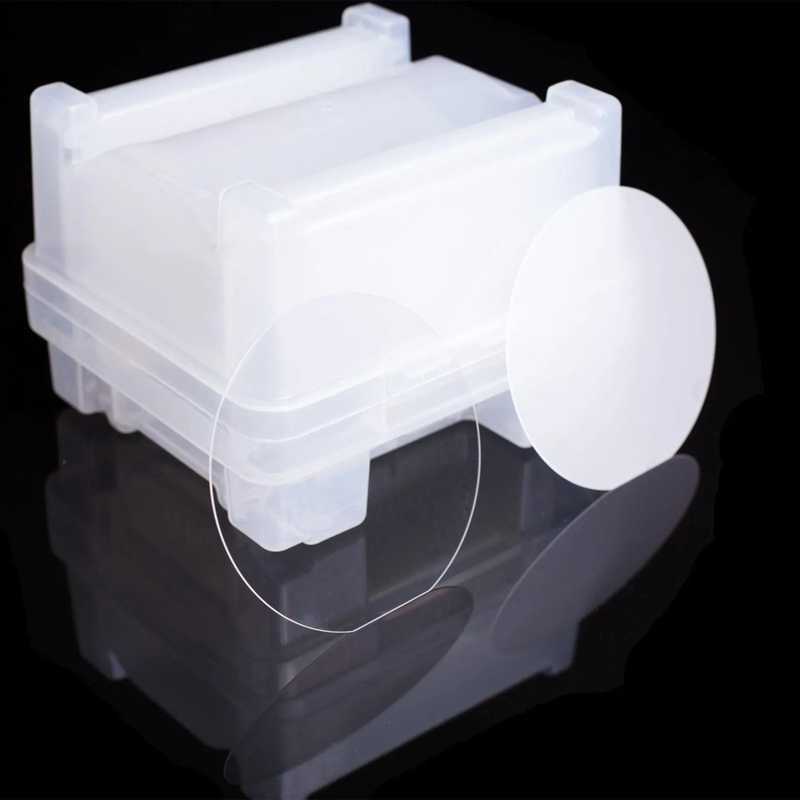
Packaging and Delivery
We provide vacuum packaging in cleanroom environments. Multi-wafer cassettes and single containers protect wafers during transport. Because reliable delivery is essential, we work with trusted global logistics partners to ensure wafers arrive safely and on time.
Conclusion and Call to Action
The sapphire wafer DSP and SSP, R-orientation (1-102) offers unique advantages for specialized epitaxy and optical applications. With Al₂O₃ ≥ 99.99%, epi-ready finishing, and strict Prime Grade quality, our wafers support both research and mass production.
If you need sapphire wafer solutions in R-plane orientation, contact our sales team today. We provide quotations, technical consultation, and secure international shipping. Because your success depends on strong substrates, we dedicate ourselves to supplying wafers that help you innovate and grow in global markets.
