
Sapphire Wafer DSP and SSP – C-Orientation Substrates for Semiconductor and Optoelectronics
Introduction
The global semiconductor and optoelectronics industries require substrates that combine mechanical strength, optical clarity, and excellent thermal stability. Traditional glass or silicon wafers cannot always deliver the required performance when engineers design advanced LEDs, lasers, and RF devices. Therefore, many manufacturers rely on sapphire wafer products because they provide the best combination of physical and chemical stability.
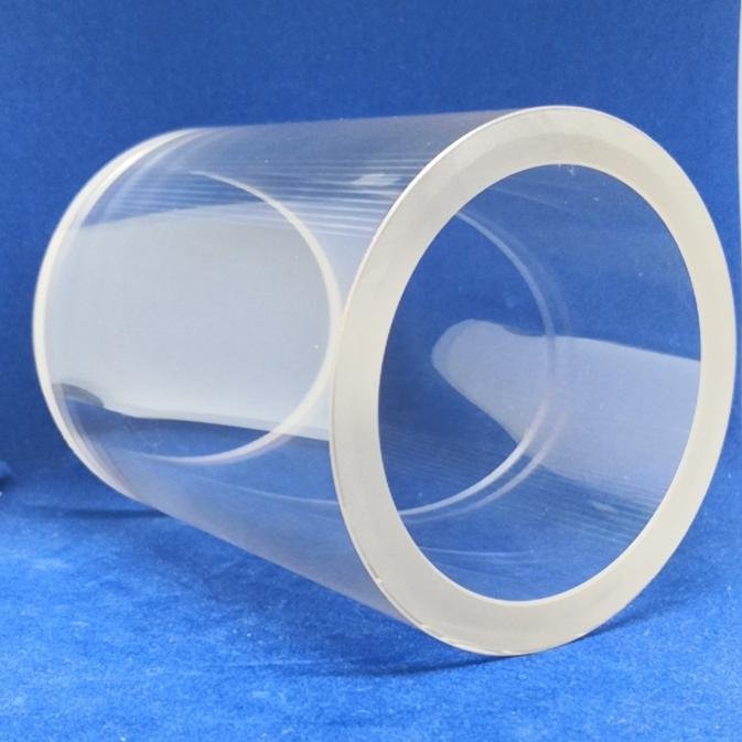
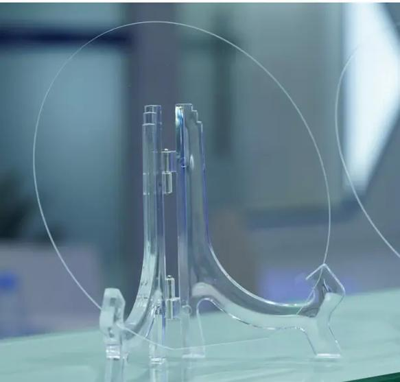
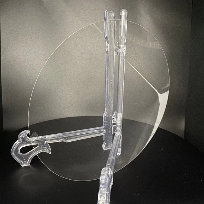
In particular, C-plane (0001) sapphire wafer has become the most widely used orientation. It supports GaN epitaxy for LED manufacturing, laser diodes, and RF power devices. Furthermore, both DSP (Double Side Polished) and SSP (Single Side Polished) versions serve different applications, giving customers flexibility for research and production.
Product Overview
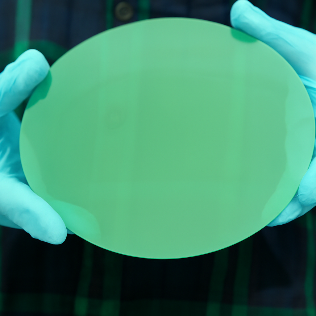
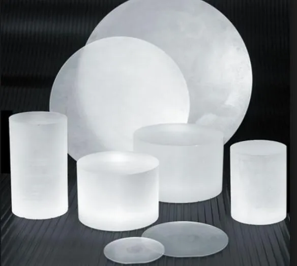
We supply sapphire wafer in DSP and SSP finishing with C-orientation (0001). DSP wafers provide polished surfaces on both sides, which improve epitaxy, optical transparency, and double-sided processing. SSP wafers provide one epi-ready surface and one lapped back surface, which reduce cost while still meeting epitaxy requirements.
Because of strict quality control, our wafers ensure consistent performance across multiple batches. Therefore, customers can rely on stable supply for both mass production and R&D activities.
Technical Specifications
The table below shows typical parameters for our sapphire wafer DSP and SSP, C-orientation (0001):
| Item | Specification |
|---|---|
| Material | Artificial sapphire (Al₂O₃ ≥ 99.99%) |
| Orientation | C-plane (0001) |
| Diameter Options | 2 inch, 4 inch, 6 inch, 8 inch, 12 inch |
| Thickness | 430 μm (2 inch), 650 μm (4 inch), 1300 μm (6–8 inch), 3000 μm (12 inch) |
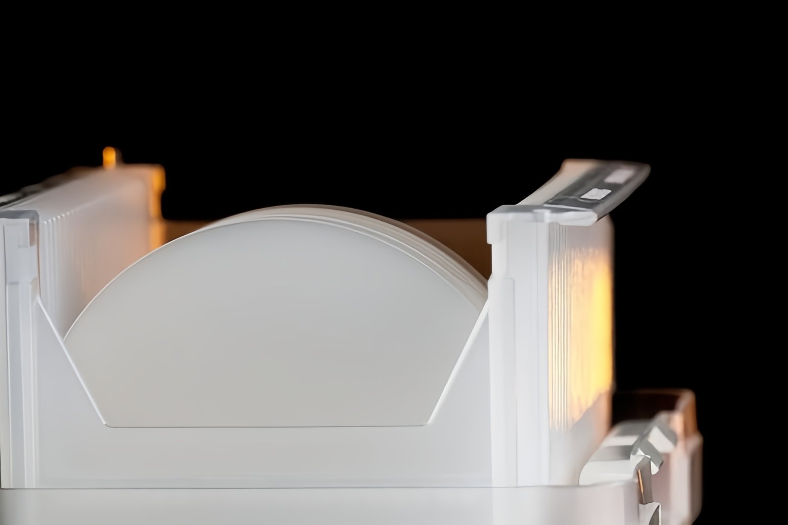
| Front Side (DSP/SSP) | DSP: Double-side polished (Ra < 0.3 nm) / SSP: Single-side polished (Ra < 0.3 nm epi-ready) |
| Back Side (DSP/SSP) | DSP: Polished / SSP: Lapped (Ra 0.6 – 1.2 μm) |
| TTV | ≤ 10 μm (2–4 inch), ≤ 15 μm (6–8 inch), negotiable for 12 inch |
| BOW | -10 ~ -25 μm depending on size |
| Warp | ≤ 15 – 30 μm depending on size |
| OF Orientation | a-plane 0 ± 0.3° |
| OF Length | 16 mm (2 inch), 30 mm (4 inch), 47.5 mm (6–8 inch), negotiable for 12 inch |
| Surface Quality | Prime Grade: Particles ≥ 0.3 μm ≤ 0.18 pcs/cm², metal contamination ≤ 2E10/cm² |
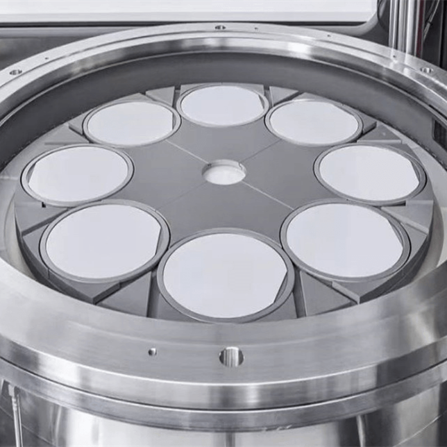
| Packaging | Vacuum packaging in cleanroom, cassette or single container |
DSP vs SSP Comparison
DSP Sapphire Wafer
Both sides polished to Ra < 0.3 nm.
Ideal for double-sided epitaxy and optical applications.
High surface uniformity improves lithography alignment.
Suitable for laser optics, advanced LED, and double-sided processing.
SSP Sapphire Wafer
Front side epi-ready with Ra < 0.3 nm.
Back side lapped with Ra 0.6 – 1.2 μm.
Cost-effective option for LED and RF epitaxy.
Suitable for mass production where only one polished side is required.
Because both options serve different needs, customers can select DSP for advanced optical or high-end devices and SSP for cost-sensitive production.
Advantages of Our Sapphire Wafer
Choosing our sapphire wafer DSP and SSP brings multiple advantages:
High Purity Material: Artificial sapphire Al₂O₃ ≥ 99.99% guarantees consistent quality.
Surface Quality: Epi-ready polishing supports defect-free GaN growth.
Orientation Stability: C-plane (0001) ensures excellent lattice matching for GaN epitaxy.
Size Flexibility: Available in 2, 4, 6, 8, and 12 inch diameters.
Cost Efficiency: SSP option reduces cost while DSP supports advanced processing.
Packaging Reliability: Cleanroom vacuum packaging ensures wafers remain free of contamination.
Moreover, customers benefit from stable supply chains, strict inspection, and technical support from our professional team.
Applications
The sapphire wafer DSP and SSP (C-orientation) supports a wide range of industries:
LED Manufacturing: GaN-on-sapphire epitaxy remains the standard for blue and white LEDs.
Laser Diodes: Optical-grade wafers support high-power laser devices.
RF and Power Devices: GaN HEMTs and RF amplifiers benefit from low-defect sapphire wafers.
Optical Windows: Transparent sapphire provides durability and optical clarity.
Consumer Electronics: Scratch-resistant sapphire components enhance watches and sensors.
Research and Universities: SSP wafers allow affordable testing, while DSP supports advanced R&D.
Because of these diverse applications, sapphire wafers continue to play a central role in modern electronics.
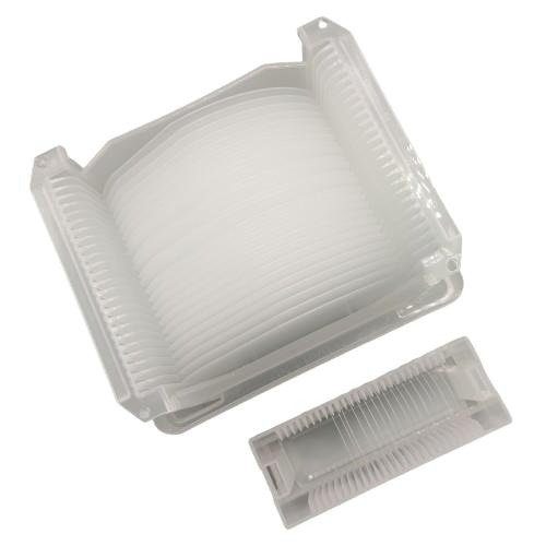
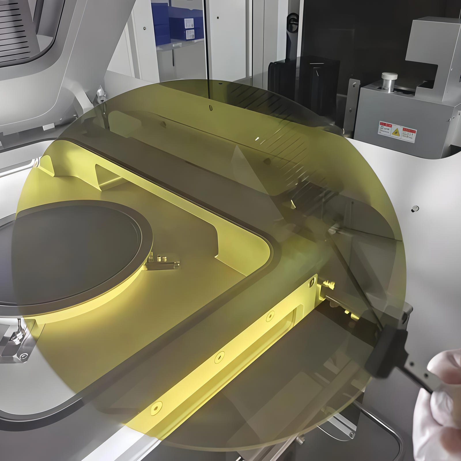
Packaging and Delivery
Every sapphire wafer undergoes vacuum packaging inside a cleanroom. Multi-wafer cassettes and single containers protect the wafers from mechanical stress and contamination. Therefore, wafers arrive ready for immediate use. Because global customers need reliable logistics, we ensure on-time delivery with trusted carriers.
Conclusion and Call to Action
The sapphire wafer DSP and SSP, C-orientation (0001) delivers unmatched reliability for semiconductor, optoelectronic, and optical applications. With Al₂O₃ ≥ 99.99%, epi-ready finishing, and strict Prime Grade standards, our wafers support both mass production and research.
If you need sapphire wafer solutions in DSP or SSP finishing, contact our sales team today. We provide fast quotations, technical consultation, and secure worldwide delivery. Because your success depends on strong substrates, we dedicate ourselves to providing wafers that help you innovate and lead your market.