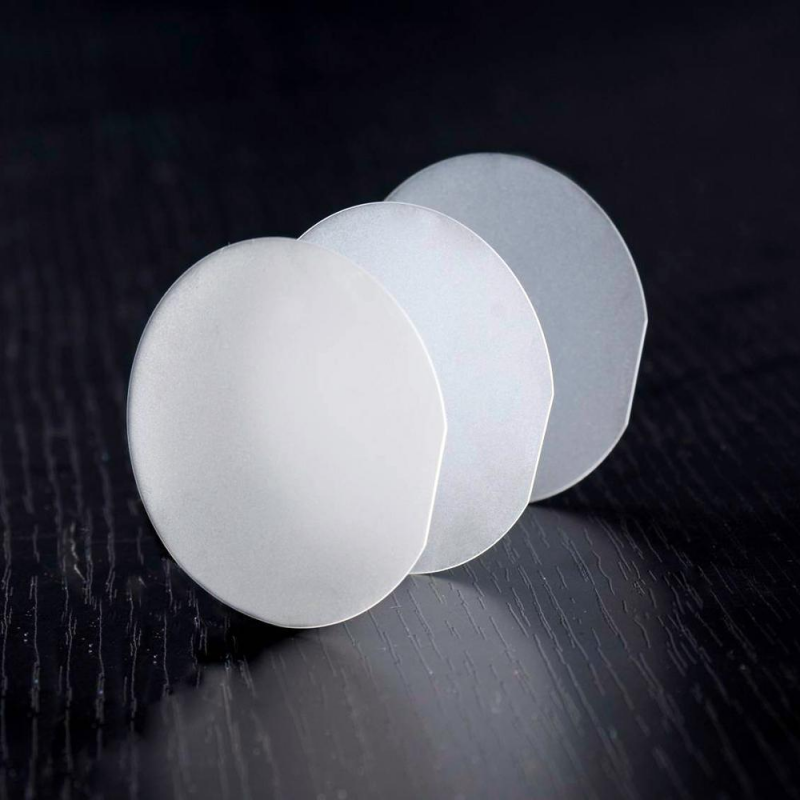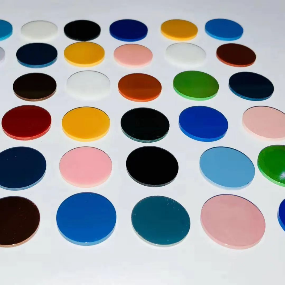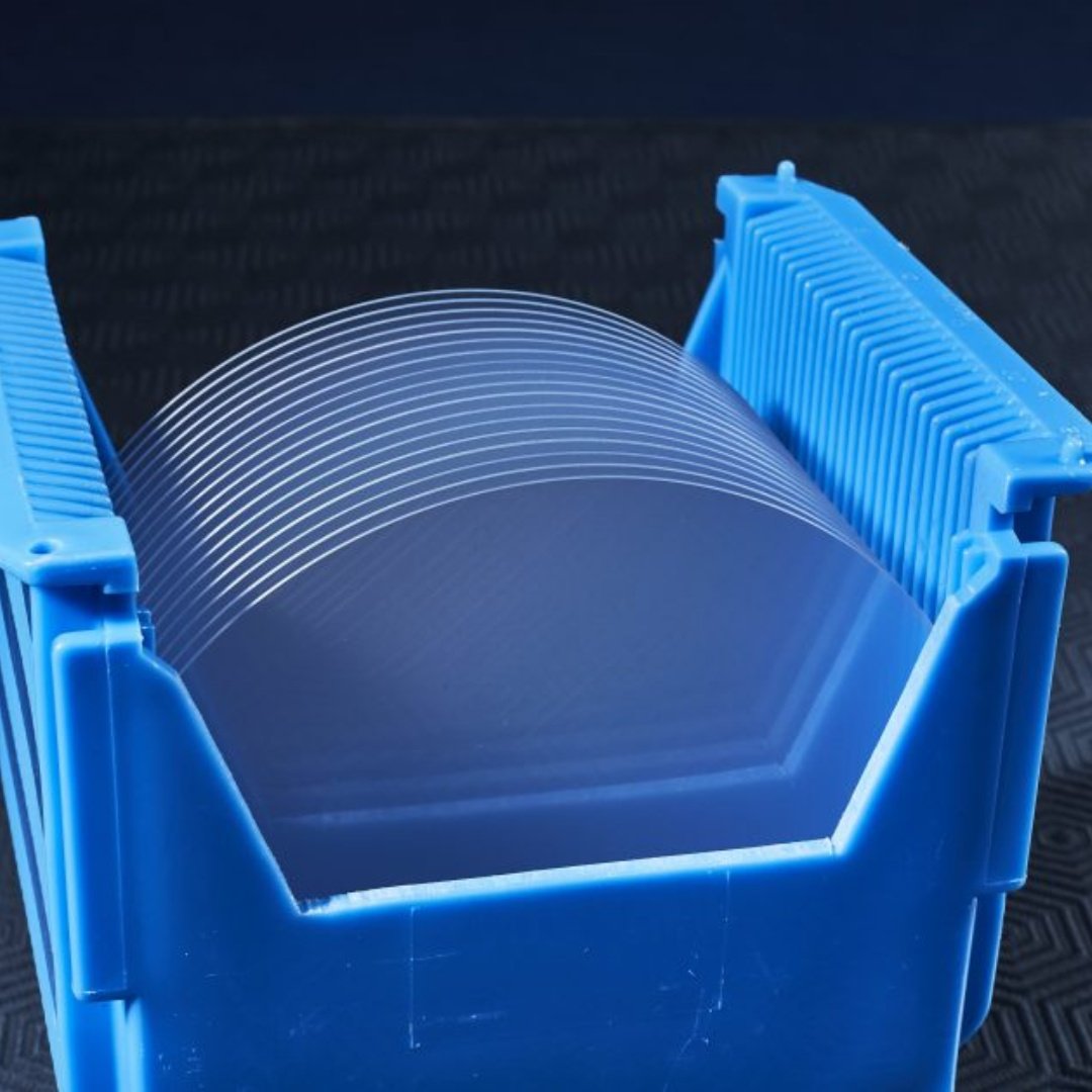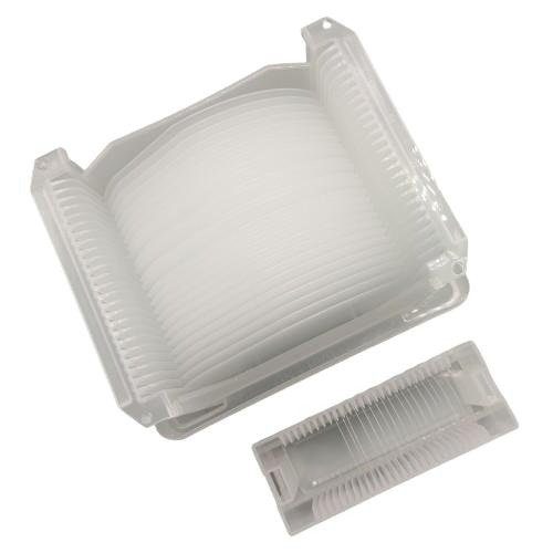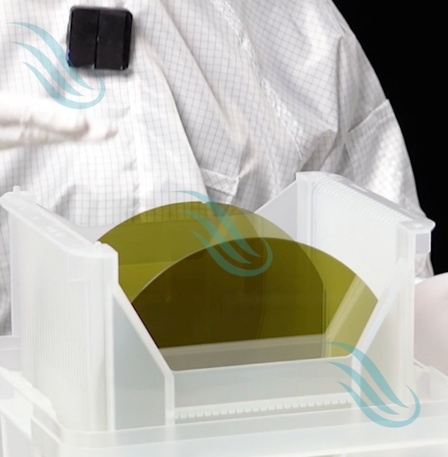

8-Inch Sapphire Substrate (Al₂O₃) – Enlarged Platform for High-Volume Optoelectronics
You pursue top-level production when you choose the sapphire wafer in an 8-inch form. You gain a substrate that integrates unmatched hardness, broad optical transparency, thermal stability, and strong electrical insulation. Because the 8‑inch sapphire substrate allows you to scale epitaxial processes, you drive volume while maintaining quality. Moreover, sapphire wafer remains a trusted foundation for GaN‑based LEDs, laser diodes, and RFICs.
You benefit from its expanded surface area, which increases throughput and lowers cost per unit. You also rely on its high purity (≥ 99.999% Al₂O₃), and you enjoy clean, polished surfaces that support defect‑free epitaxy. Meanwhile, sapphire wafer survives extreme environments, and you apply it across UV to IR optical systems. In essence, sapphire wafer enables your industrial ambitions without compromising precision.
Why the 8-Inch Sapphire Wafer Delivers
You achieve industrial scalability through the 8‑inch sapphire wafer. Compared with smaller formats, you reduce per‑unit cost and increase throughput. Compared with larger formats, you maintain equipment compatibility and enjoy wider supplier availability.
You rely on sapphire’s rank‑9 hardness to protect your devices from scratches and contamination. You also leverage its wide spectral transmission—from ultraviolet through infrared—to support advanced optical components. Additionally, sapphire wafer provides low dielectric loss and high dielectric strength, so you ensure stable high‑frequency performance.
Key Features of Sapphire Wafer
Ultra‑high purity (single‑crystal Al₂O₃ ≥ 99.999%) ensures consistent crystal quality.
Large 200 mm diameter supports high‑volume manufacturing.
Epi‑ready polished surfaces (Ra < 0.2 nm) promote smooth epitaxy.
Thermally stable beyond 1000 °C, so you handle intense processing.
Broad optical transparency (200 nm to 5 µm) accommodates UV to IR systems.
Strong electrical insulation and low dielectric loss strengthen RF performance.
Mohs hardness of 9 provides long‑term durability in harsh environments.
Technical Specification Table: 8-Inch Sapphire Wafer
| Parameter | Specification (Typical) |
|---|---|
| Material Purity | ≥ 99.999% monocrystalline Al₂O₃ finewinwafers.com+7CRYSCORE+7orbray.com+7CRYSCORE |
| Diameter | 200.0 mm ± 0.2 mm ≈ 8 inch CRYSCOREKYOCERA |
| Thickness | 1300 µm ± 25 µm (common), also 1500 µm option CRYSCORE+1 |
| Surface Finish (SSP / DSP) | SSP: front epi-polished Ra < 0.2 nm, back fine ground Ra ≈ 0.8–1.2 µm; DSP: both polished Ra < 0.2 nm CRYSCORE |
| TTV / Bow / Warp | < 30 µm each CRYSCORE |
| Orientation | C-plane (0001) standard (off-angle ±0.2° possible) CRYSCORE |
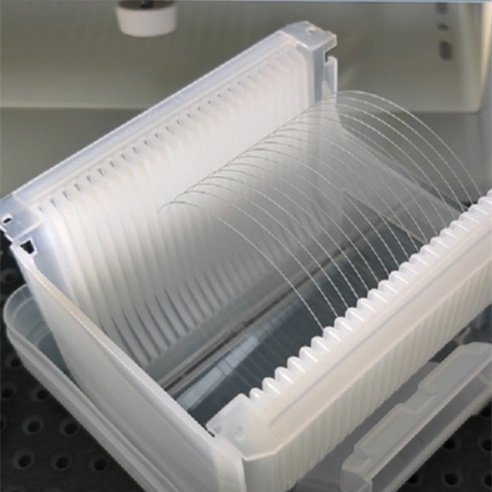
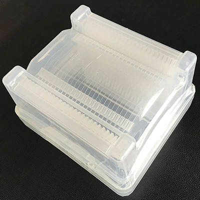
| Packaging | Class-100 cleanroom cleaning, vacuum cassette CRYSCORE+1 |
| Thermal Expansion Coefficient | ‖ C-axis: 6.66×10⁻⁶ /°C; ⟂ C-axis: 5×10⁻⁶ /°C CRYSCOREFirebird Optics |
| Thermal Conductivity | ≈ 40 W/(m·K) at 20 °C Firebird OpticsCRYSCORE |
| Dielectric Constant | ≈ 11.5 (‖ C-axis), ≈ 9.3 (⟂ C-axis) at 1 MHz CRYSCOREFirebird Optics |
| Dielectric Strength | ≈ 4.8×10⁵ V/cm CRYSCOREFirebird Optics |
| Dielectric Loss (tan δ) | < 1×10⁻⁴ CRYSCOREFirebird Optics |
| Refractive Index | ~1.77 (visible) Firebird Optics |
| Optical Transmission | ~88% @460 nm, broad UV–IR transparency Firebird Opticsuniversitywafer.com |
| Hardness | Mohs 9 |
Applications of 8-Inch Sapphire Substrate
1. LED and GaN Epitaxy
You scale LED production effectively on 8-inch sapphire wafer. Because GaN grows reliably on C-plane sapphire, you increase yields and reduce costs in blue, green, and UV LED manufacturing.
2. Laser Diodes and Photonic Devices
You employ sapphire wafer in UV–IR laser systems and photonic components. Its optical clarity and polish support stable optical performance in high-demand systems.
3. RFIC and Silicon-on-Sapphire (SOS) Circuits
You base RFIC and SOS devices on sapphire wafer. Its dielectric properties and electrical insulation suit high-frequency and RF performance.
4. Optical Windows and Sensors
You craft large-diameter optical windows and sensors from sapphire substrate. Its transparency, scratch-resistance, and thermal reliability make it ideal for cameras, aerospace optics, and vacuum viewports MSE Supplies LLC+7universitywafer.com+7CRYSCORE+7universitywafer.com.
5. High-Volume Research & Pilot Lines
You test new processes at scale using 8-inch sapphire wafer. It bridges lab and production, so you pilot materials and aligns with mass production from the start.
Production Methods and Customization
Manufacturers grow sapphire boules using Kyropoulos (KY), Czochralski (CZ), or EFG methods. They cut, grind, and polish wafers to precise dimensions. You receive sapphire wafer with polished surfaces (epi‑ready Ra < 0.2 nm) via CMP processes. Meanwhile, suppliers offer customization—orientation flats, miscut angles, thickness variations, and patterned surfaces—so you tailor sapphire substrate exactly to your device needs Firebird Optics+1.
Why Sapphire Wafer Outperforms Other Substrates
You compare sapphire wafer with silicon, SiC, or quartz. While silicon cannot withstand high-temperature or provide optical transmission, sapphire does both. SiC can be costly and conductive, whereas sapphire offers cheaper optical transparency. Quartz lacks hardness and dielectric strength. Therefore, sapphire wafer uniquely combines durability, transparency, dielectric performance, and scalability.
Conclusion
When you adopt the 8-inch sapphire wafer, you invest in a substrate that supports industrial-scale production, high optical fidelity, and high-frequency device use. You ensure consistency, purity, and yield, while leveraging broad spectrum transparency and mechanical strength. You position your manufacturing to thrive—and sapphire wafer delivers.
Q&A: Centered on “Sapphire Wafer”
Q: Why choose 8-inch sapphire wafer over smaller sizes?
A: You achieve higher throughput, lower cost per device, and seamless scale-up from R&D to production—while keeping material quality intact.
Q: Does polishing type matter for sapphire wafer?
A: Yes—you select SSP if you need only one epi-ready face; you use DSP when both sides must support optical processing or dual-sided growth.
Q: Can the sapphire wafer sustain high-temperature fabrication?
A: Absolutely—you rely on sapphire’s ability to stay stable above 1000 °C and resist thermal shock even in aggressive processes.
Q: How does sapphire compare with silicon or SiC?
A: You benefit from sapphire’s optical clarity and hardness, which silicon lacks, and its lower cost and transparency relative to SiC.
Q: Are customization options available for 8-inch sapphire substrates?
A: Definitely—you specify flats, off-angles, thickness, orientation, or surface patterns to tailor sapphire wafer precisely for your application.