
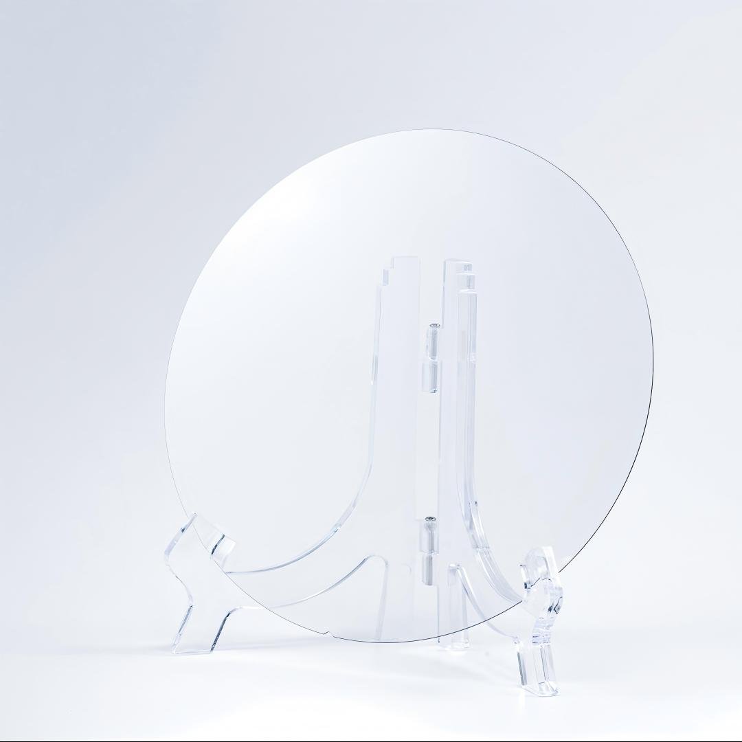
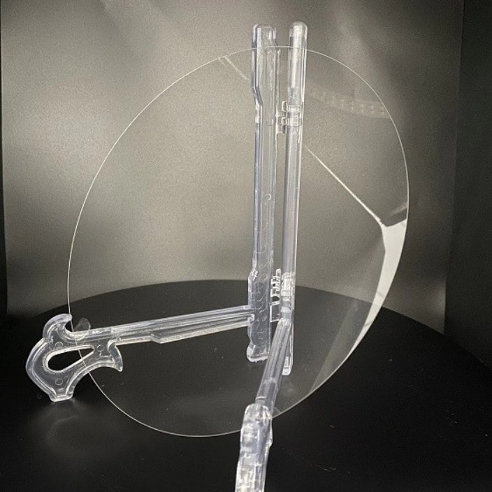
Sapphire Wafer 8 Inch C-Plane – Product Introduction
Overview
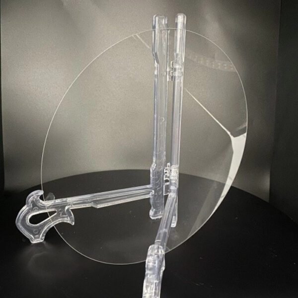
A sapphire wafer 8 inch C-plane represents the next generation of large-diameter substrates for semiconductor, LED, and optical applications. Sapphire, chemically defined as Al₂O₃, has gained global recognition for its unmatched hardness, superior thermal conductivity, and wide optical transmission range from ultraviolet to infrared. With the C-plane orientation (0001), this wafer delivers a stable lattice structure that ensures reliable GaN epitaxy and consistent device performance.
As the industry shifts from 4 inch and 6 inch wafers to larger diameters, the 8 inch sapphire wafer provides greater scalability. Because more devices can be processed on a single wafer, manufacturers achieve higher throughput, lower cost per chip, and improved efficiency. Therefore, the sapphire wafer 8 inch C-plane has become the benchmark substrate for companies that want to expand production capacity while maintaining the highest quality standards.
Key Advantages of Sapphire Wafer 8 Inch C-Plane
High Throughput: Larger surface area allows more chips per wafer, which reduces unit cost.
Hardness and Durability: Mohs hardness 9 resists scratches, cracks, and wear during processing.
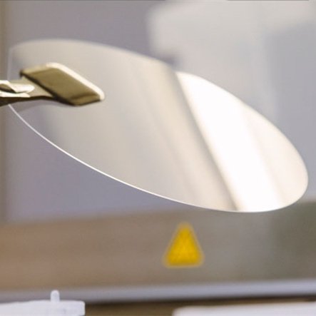
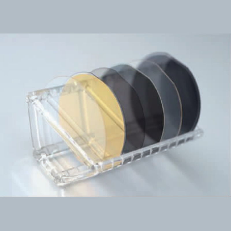
Excellent Optical Properties: Transparency from 200 nm (UV) to 5000 nm (IR).
Thermal Stability: Withstands high-temperature epitaxial processes without deformation.
Chemical Resistance: Maintains performance under aggressive cleaning and etching conditions.
C-plane Orientation: Provides a perfect lattice template for GaN epitaxy and LED structures.
Precise Surface Quality: Tight tolerances on TTV, BOW, and WARP ensure consistent device yield.
Because of these features, the 8 inch sapphire wafer is not only a scaling step but also a technological leap toward more efficient manufacturing.
Technical Specifications – Sapphire Wafer 8 Inch C-Plane
| Item | Specification |
|---|---|
| Diameter | 8 inch (200 mm ± 0.5 mm) |
| Material | Monocrystalline Al₂O₃ (≥ 99.999%) |
| Crystal Orientation | C-plane (0001) |
| Orientation Accuracy | ±0.3° |
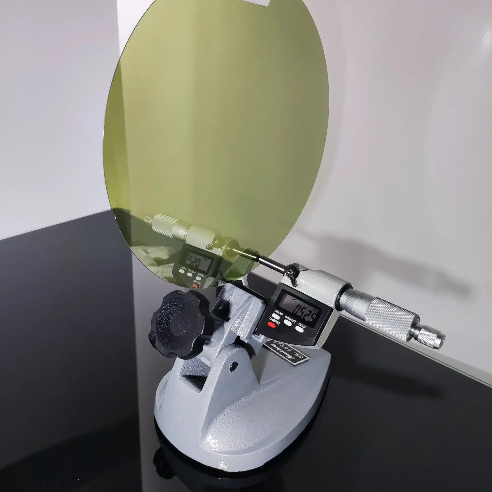
| Thickness | 1300 ± 20 µm |
| Primary Flat (OF) | 47.5 ± 2.5 mm |
| OF Orientation | A-plane (11-20) |
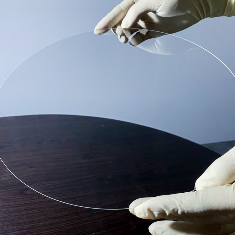
| Surface Type | SSP (Single-Side Polished) / DSP (Double-Side Polished) |
| Surface Roughness | Ra ≤ 0.3 nm (DSP) |
| TTV | ≤ 15 µm |
| BOW | ≤ 25 µm |
| WARP | ≤ 25 µm |
| Edge Profile | Rounded or beveled (custom available) |
| Packaging | Class 100 cleanroom, wafer cassette, vacuum sealed |
Applications of Sapphire Wafer 8 Inch C-Plane
1. LED Production
The 8 inch sapphire wafer enables cost-effective GaN-on-sapphire epitaxy. Because more chips fit on one wafer, LED manufacturers reduce cost per lumen and increase output capacity.
2. Power Electronics and RF Devices
GaN-based RF power amplifiers and power switches require substrates that support high-frequency stability. The 8 inch sapphire wafer provides large-area processing and better scalability.
3. Optical and Infrared Components
Sapphire’s transparency from UV to IR makes it suitable for protective covers, infrared windows, and precision optical components used in aerospace, defense, and scientific instruments.
4. Laser Systems
Medical lasers, high-power industrial lasers, and optical diagnostic systems use sapphire wafers for their durability and resistance to extreme energy loads.
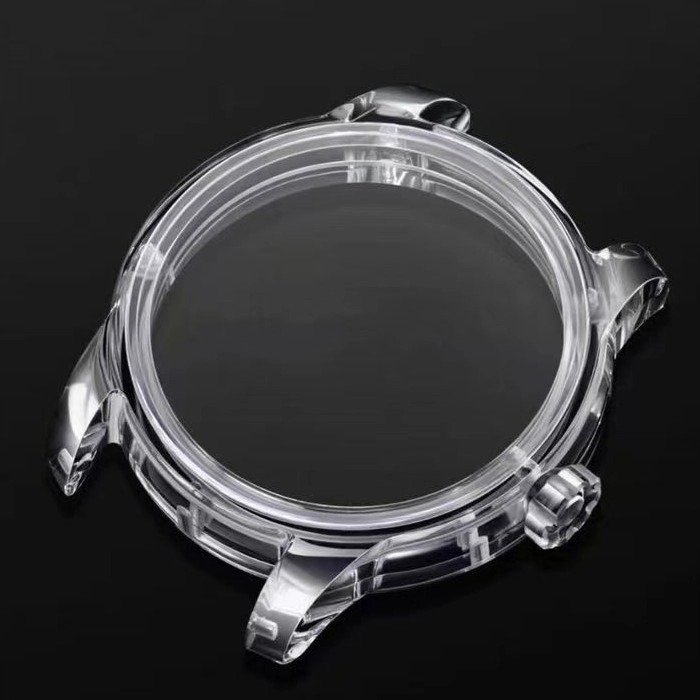
5. Consumer Electronics
Premium smartphones, smartwatches, and wearable devices integrate sapphire components such as camera lenses and micro-optical windows to ensure durability and luxury design.
Application Summary
A sapphire wafer 8 inch C-plane offers the best combination of cost reduction and scalability for modern optoelectronics. With its large diameter, it enables higher throughput in LED fabs, reliable epitaxy for GaN power devices, and premium durability for optical and consumer electronics. The wafer’s outstanding thermal and mechanical properties make it essential for next-generation mass production.
Because it supports multiple industries simultaneously, the sapphire wafer 8 inch is not only a substrate but also a growth driver for global technology markets.
Q&A Section
Q1: Why move from 6 inch to 8 inch sapphire wafers?
A: The 8 inch wafer offers a larger processing area. This reduces chip cost, increases throughput, and enables better economies of scale in LED and RF device manufacturing.
Q2: Why is the C-plane orientation important?
A: The C-plane (0001) provides the most suitable lattice match for GaN epitaxial growth. It minimizes dislocation density and enhances device reliability.
Q3: Do you provide custom thickness or edge profiles?
A: Yes. Thickness, edge rounding, and bevel profiles can be fully customized to meet specific requirements.
Q4: Can you supply DSP wafers for epitaxy?
A: Yes. DSP wafers are available and deliver ultra-flat surfaces required for advanced epitaxial growth.
Q5: How do you guarantee wafer flatness and quality?
A: Every wafer passes strict metrology inspections, including TTV, BOW, and WARP measurements. Our polishing lines ensure consistent high quality.
Q6: Which industries mostly purchase 8 inch sapphire wafers?
A: LED manufacturers, GaN semiconductor companies, defense optics suppliers, and consumer electronics brands.
Q7: How does sapphire compare to SiC wafers?
A: SiC wafers target high-power MOSFETs, while sapphire wafers remain cost-effective for LEDs, RF devices, and optical components. Sapphire also offers superior optical transparency.
Q8: How are the wafers packaged for safe shipping?
A: Wafers are packed in cleanroom wafer cassettes, vacuum sealed, and protected with ESD-safe, shock-proof cartons to ensure defect-free delivery.
Conclusion
The sapphire wafer 8 inch C-plane is the foundation for high-volume LED production, GaN power electronics, and advanced optical systems. With its hardness, optical clarity, and scalability, it outperforms smaller-diameter wafers in terms of cost efficiency and manufacturing throughput.
By selecting a sapphire wafer 8 inch C-plane, manufacturers gain a reliable substrate that supports both current production and future expansion. As global industries continue to scale up, the 8 inch wafer will remain the preferred choice for companies that value quality, performance, and efficiency.
