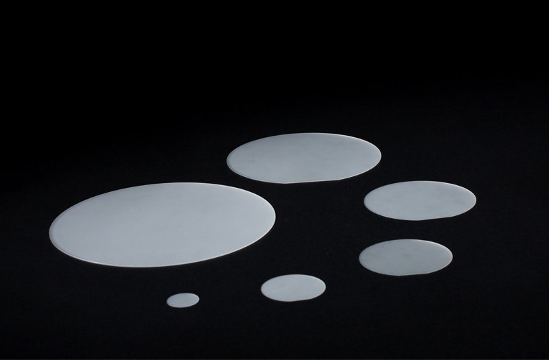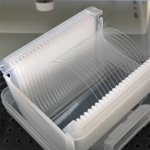

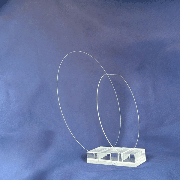
Sapphire Wafer 4 Inch C-Plane – Product Introduction
Overview
A sapphire wafer 4 inch C-plane plays an essential role in semiconductor, LED, and optical applications. Sapphire, known chemically as Al₂O₃, offers exceptional hardness, outstanding thermal conductivity, and remarkable optical transmission from ultraviolet to infrared. The C-plane orientation (0001) provides a stable and uniform substrate surface, which enables reliable epitaxial growth of GaN and other compound semiconductors.
Because of its unique physical and chemical stability, a 4 inch sapphire wafer meets the requirements of both research laboratories and large-scale industrial production lines. Moreover, the wafer maintains high surface quality, precise thickness control, and consistent crystallographic orientation, which ensures better device performance.
In the global market, engineers and manufacturers choose sapphire wafers as their preferred substrate because they want durability, transparency, and compatibility with modern processing equipment. As a result, sapphire wafer 4 inch C-plane has become the standard size for many optoelectronic and microelectronic industries.
Key Advantages of Sapphire Wafer 4 Inch C-Plane
High Hardness: Mohs hardness level 9, second only to diamond.
Wide Transmission Range: From 200 nm (UV) to 5000 nm (IR).
Excellent Thermal Properties: High thermal conductivity and resistance to thermal shock.
Chemical Resistance: Stable against most acids and alkalis, enabling long-term reliability.
Dimensional Precision: Tight control on TTV, BOW, and WARP ensures high-yield processing.
Surface Orientation: C-plane (0001) orientation offers an ideal lattice structure for GaN-based LEDs and RF devices.
With these benefits, sapphire wafers improve device lifetime, production yield, and final product stability.
Technical Specifications – Sapphire Wafer 4 Inch C-Plane
| Item | Specification |
|---|---|
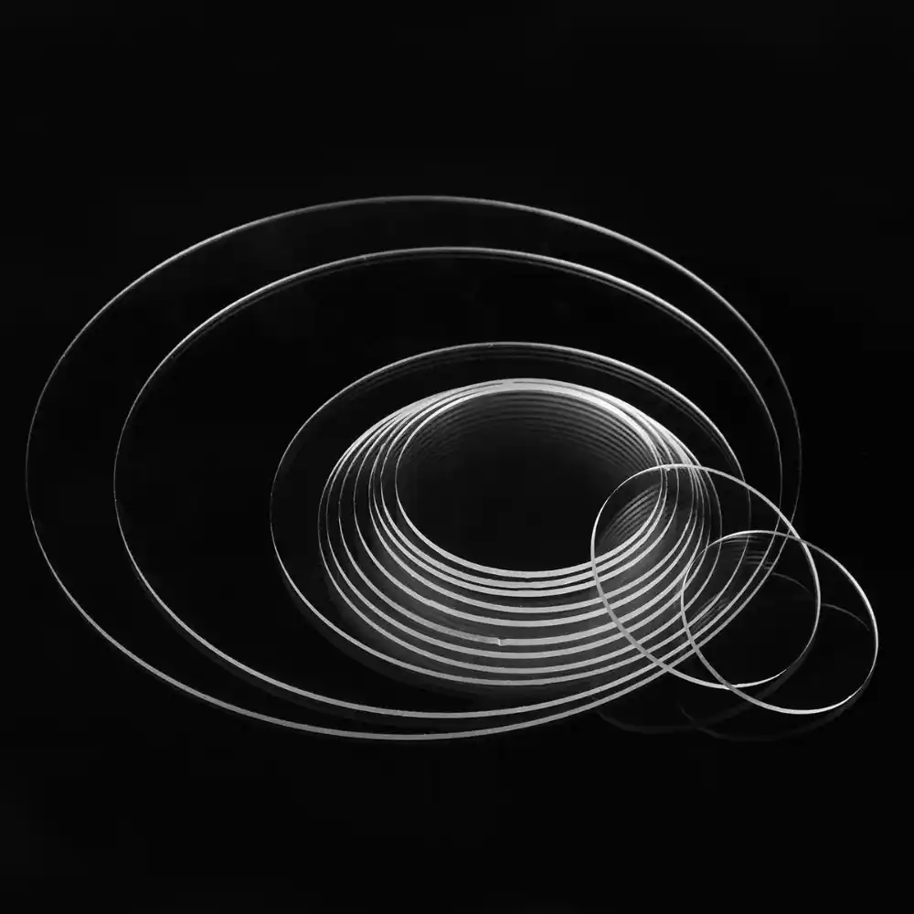
| Diameter | 4 inch (100 mm ± 0.5 mm) |
| Material | Monocrystalline Al₂O₃ (≥ 99.999%) |
| Crystal Orientation | C-plane (0001) |
| Orientation Accuracy | ±0.3° |
| Thickness | 650 ± 15 µm |
| Primary Flat (OF) | 30 ± 1 mm |
| OF Orientation | A-plane (11-20) |
| Surface Type | SSP (Single-Side Polished) / DSP (Double-Side Polished) |
| Surface Quality | Ra ≤ 0.3 nm (DSP) |
| TTV (Total Thickness Variation) | ≤ 10 µm |
| BOW | ≤ 15 µm |
| WARP | ≤ 15 µm |
| Edge Profile | Rounded or beveled (custom available) |
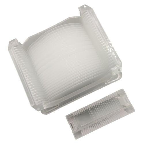
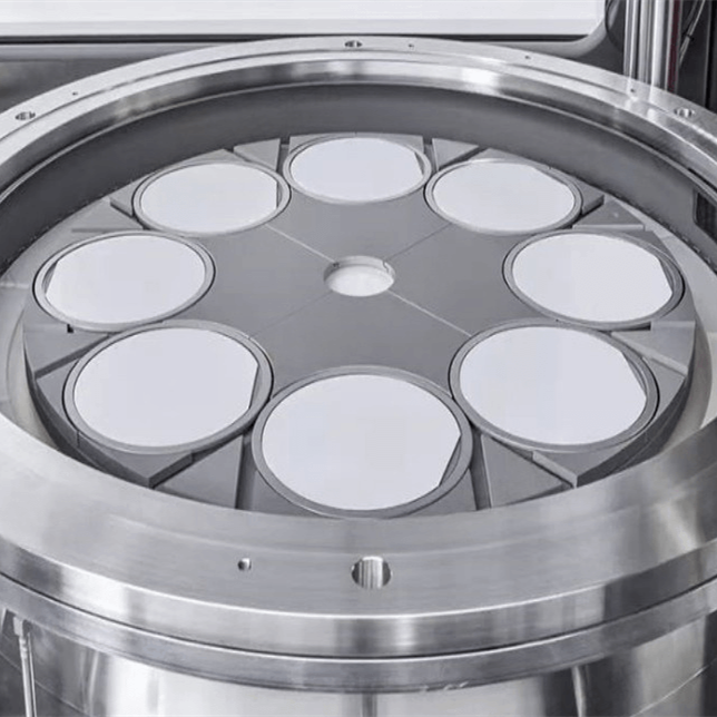
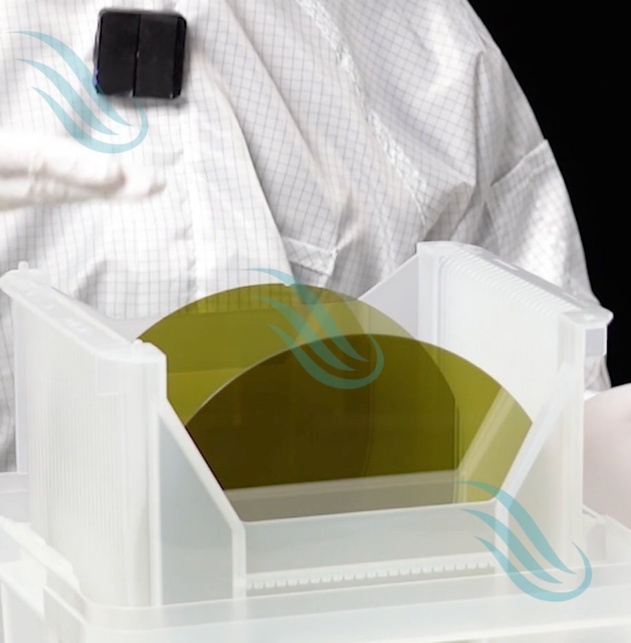
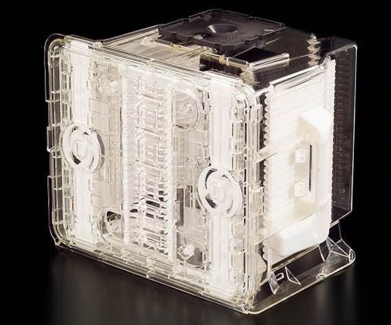
| Packaging | Class 100 cleanroom, wafer cassette, vacuum sealed |
Applications of Sapphire Wafer 4 Inch C-Plane
The sapphire wafer 4 inch C-plane supports diverse industries because of its unmatched versatility.
1. LED Manufacturing
The wafer provides the perfect substrate for GaN-based LED growth. The stable lattice match between sapphire and GaN improves crystal quality, which leads to higher luminous efficiency and longer device life.
2. Optical Windows and Lenses
Sapphire’s wide optical transmission and scratch resistance make it an ideal material for UV–IR optical windows, protective covers, and high-precision lenses.
3. Semiconductor Devices
In RFICs and power electronics, sapphire substrates reduce parasitic capacitance, improve device isolation, and maintain consistent high-frequency performance.
4. Medical and Laser Systems
High-purity sapphire offers low absorption and excellent resistance to high-power lasers, which makes it ideal for laser optics and medical diagnostic systems.
5. Consumer Electronics
Smartphone covers, watch crystals, and camera lenses benefit from sapphire’s durability and transparency.
Because of these wide-ranging uses, a sapphire wafer ensures continuous demand in industries that rely on both performance and reliability.
Application Summary
The sapphire wafer 4 inch C-plane stands as the backbone of advanced optoelectronic technology. Manufacturers use it for GaN epitaxy in LED production, ensuring brilliant light output and long service life. Researchers apply it in semiconductor experiments, where they need high precision and chemical resistance. Optical industries choose sapphire wafers for UV and IR windows, ensuring maximum transmission and durability.
Therefore, one wafer serves multiple sectors. This cross-industry compatibility guarantees stable market demand and positions the sapphire wafer 4 inch C-plane as an indispensable material in both present and future technologies.
Q&A Section
Q1: Why should I choose a sapphire wafer instead of other substrates?
A: A sapphire wafer offers unmatched hardness, excellent optical transmission, and superior chemical stability. These qualities provide longer device life, higher yield, and better resistance to environmental challenges compared with alternatives like Si or quartz.
Q2: What does C-plane orientation mean?
A: The C-plane orientation (0001) refers to the crystallographic direction of the sapphire wafer. This orientation provides an ideal surface for GaN epitaxial growth, making it the standard choice for LED and RF device production.
Q3: Can I request custom thickness or edge profiles?
A: Yes, we offer full customization. Clients can specify thickness, bevel type (R/T), edge rounding, and even surface roughness to match unique processing requirements.
Q4: How do you package sapphire wafers for shipping?
A: We package all wafers in cleanroom environments. Each batch is vacuum-sealed inside wafer cassettes with ESD protection and then placed in shock-proof outer cartons. This ensures wafers arrive in perfect condition.
Q5: Are both SSP and DSP available for the 4 inch wafer?
A: Yes, we provide both SSP and DSP options. SSP fits cost-sensitive projects, while DSP ensures ultra-flat surfaces for precision epitaxy.
Q6: What industries commonly purchase 4 inch sapphire wafers?
A: LED manufacturers, semiconductor companies, optical labs, laser system suppliers, and consumer electronics brands are frequent buyers of sapphire wafers.
Q7: How does sapphire compare with fused silica or quartz wafers?
A: Unlike fused silica, sapphire is crystalline, harder, and more thermally stable. Quartz is cheaper but lacks sapphire’s hardness and lattice compatibility with GaN. Therefore, sapphire remains the best choice for high-end semiconductor and optical applications.
Q8: Can you support bulk production for large projects?
A: Absolutely. Our production lines include KY furnaces, precision multi-wire saws, and double-side grinders, which ensure consistent quality across large-volume orders.
Conclusion
A sapphire wafer 4 inch C-plane is more than just a substrate. It is the foundation of LED technology, semiconductor devices, and optical components. With superior hardness, optical clarity, and thermal stability, sapphire wafers continue to dominate industries that require both performance and durability.
Whether you need wafers for research, mass production, or optical engineering, our sapphire wafers deliver reliable results every time. By choosing a sapphire wafer 4 inch C-plane, you ensure that your devices operate with greater efficiency, longer lifetime, and higher yield.