
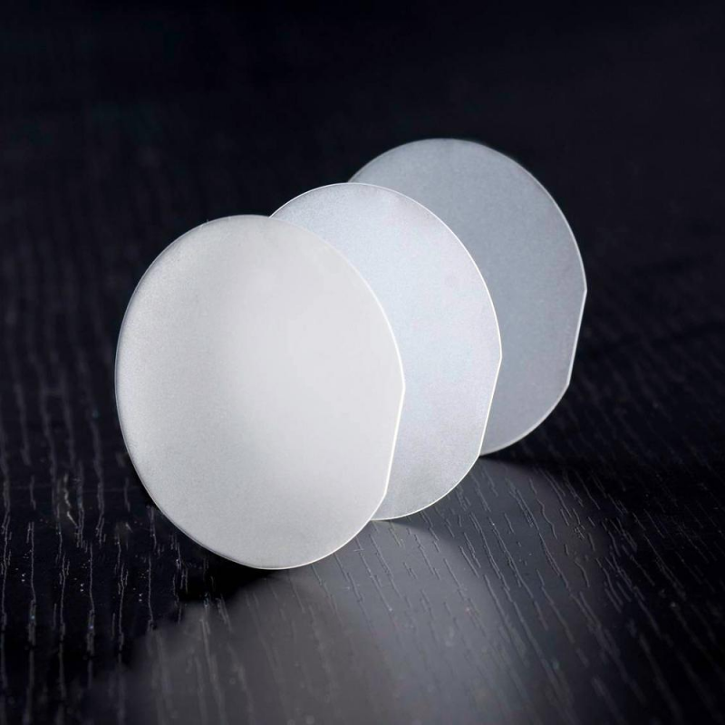
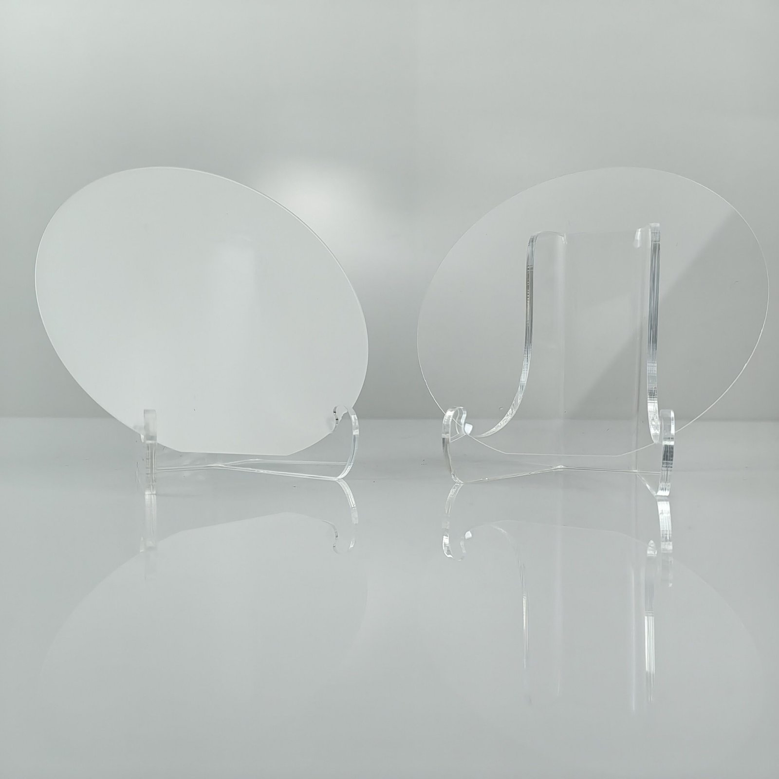
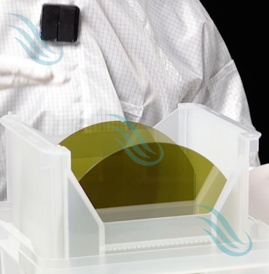
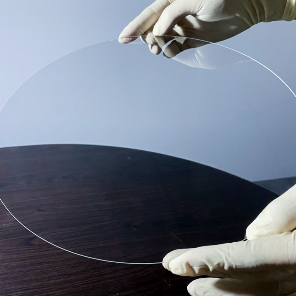
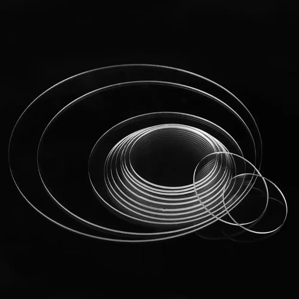
Sapphire Wafer 4-Inch & 6-Inch (500 µm) – High Purity Al₂O₃ Substrates
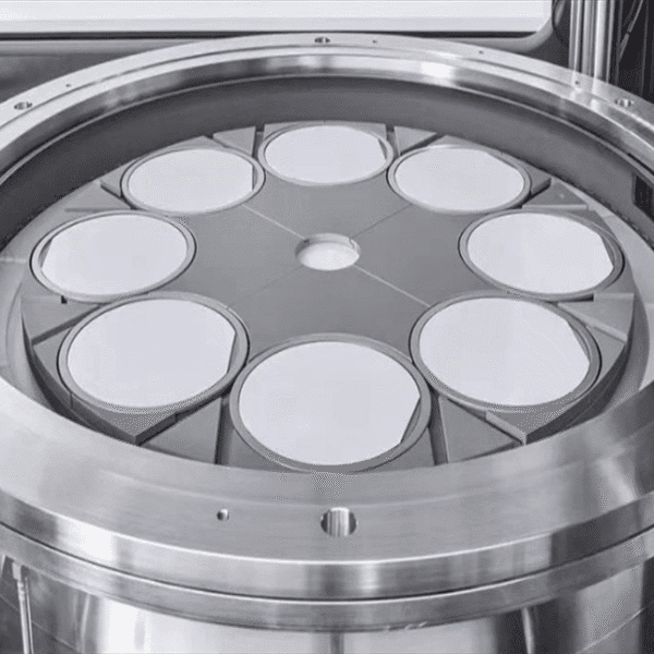
The sapphire wafer continues to dominate as a critical material in modern semiconductor and photonic applications. When you choose sapphire wafer in 4-inch and 6-inch formats with 500 µm thickness, you gain a substrate that integrates excellent thermal stability, wide-spectrum optical transmission, extreme hardness, and strong electrical insulation. Because sapphire substrate combines these properties, it delivers reliability from laboratory research to mass production.
You rely on sapphire wafer to enhance epitaxy of GaN, LEDs, RFICs, MEMS, and photonic devices. With 500 µm thickness, you maintain a balance between strength and process compatibility. The 4-inch size supports flexible prototyping, while the 6-inch format delivers higher throughput. You achieve cost efficiency, and you expand applications without sacrificing material quality.
Why Sapphire Wafer 4-Inch & 6-Inch, 500 µm Excels
You select the sapphire wafer because it offers consistent purity and crystal quality. You benefit from ≥ 99.99% Al₂O₃ single crystal, so you minimize dislocations during epitaxial growth. You also exploit the wafer’s Mohs hardness of 9, which ensures long service life. Moreover, you take advantage of sapphire’s transparency across UV to IR, which makes it indispensable in lasers, detectors, and optical windows.
You rely on sapphire wafer because it withstands > 1000 °C processing. You use it confidently in environments that would damage silicon or quartz. Furthermore, you reduce dielectric loss in RF devices because sapphire delivers low loss tangent and high dielectric strength. You also exploit dimensional stability, with bow and warp typically < 15 µm, so you secure uniform epitaxy and higher yields.
Key Features
High-purity single crystal Al₂O₃ guarantees reliable epitaxy.
500 µm thickness balances strength and lightweight handling.
Polished surfaces (Ra < 0.3 nm) ensure epi-ready quality.
Thermal conductivity 30–42 W/(m·K) aids in heat dissipation.
Dielectric constant 9–11 supports RFIC and SOS applications.
Hardness Mohs 9 maintains scratch resistance and durability.
Transparency 200 nm–5 µm covers UV, visible, and IR bands.
Technical Specifications of 4-Inch and 6-Inch Sapphire Wafer (500 µm)
| Parameter | 4-Inch Sapphire Wafer | 6-Inch Sapphire Wafer |
|---|---|---|
| Material Purity | ≥ 99.99% Al₂O₃ | ≥ 99.99% Al₂O₃ |
| Diameter | 100 mm ± 0.1 mm | 150 mm ± 0.2 mm |
| Thickness | 500 µm ± 15 µm | 500 µm ± 20 µm |
| Orientation | C-plane (0001); A-, R-, M-plane optional | C-plane (0001); A-, R-, M-plane optional |
| Surface Finish | SSP or DSP; Ra < 0.3 nm | SSP or DSP; Ra < 0.3 nm |
| TTV / Bow / Warp | ≤ 10–15 µm | ≤ 15–20 µm |
| Primary Flat & Length | ~30 mm | ~47.5 mm |
| Edge Profile | SEMI bevel standard | SEMI bevel standard |
| Thermal Expansion Coefficient | ∥ C-axis: 6.66×10⁻⁶ /°C; ⟂ C-axis: 5.0×10⁻⁶ /°C | ∥ C-axis: 6.66×10⁻⁶ /°C; ⟂ C-axis: 5.0×10⁻⁶ /°C |
| Thermal Conductivity | 30–42 W/(m·K) @25 °C | 30–42 W/(m·K) @25 °C |
| Dielectric Constant | ∥ C ≈ 11.5; ⟂ C ≈ 9.3 | ∥ C ≈ 11.5; ⟂ C ≈ 9.3 |
| Dielectric Strength | ~4.8×10⁵ V/cm | ~4.8×10⁵ V/cm |
| Refractive Index | ~1.77 (visible) | ~1.77 (visible) |
| Optical Transmission | 200 nm–5 µm | 200 nm–5 µm |
| Mohs Hardness | 9 | 9 |
Applications of Sapphire Wafer 4-Inch and 6-Inch (500 µm)
LED and GaN Epitaxy
You rely on sapphire wafer to support GaN growth. With 4-inch wafers, you handle prototyping and pilot runs. With 6-inch wafers, you manage larger production, which drives cost reduction.
Lasers and Photonics
You employ sapphire wafer in UV and IR lasers, detectors, and photonic systems. Its broad optical transmission ensures efficient light propagation.
RFIC and SOS Devices
You use sapphire wafer in RFIC and silicon-on-sapphire applications. Its low dielectric loss strengthens signal reliability.
MEMS and Sensors
You integrate sapphire substrate into MEMS, sensors, and optical windows. The 500 µm thickness enhances mechanical stability.
Research and Development
You adopt sapphire wafer in 4-inch format for laboratory tests. You transition to 6-inch when scaling toward industry. This pathway reduces costs and maintains consistency.
Manufacturing and Customization
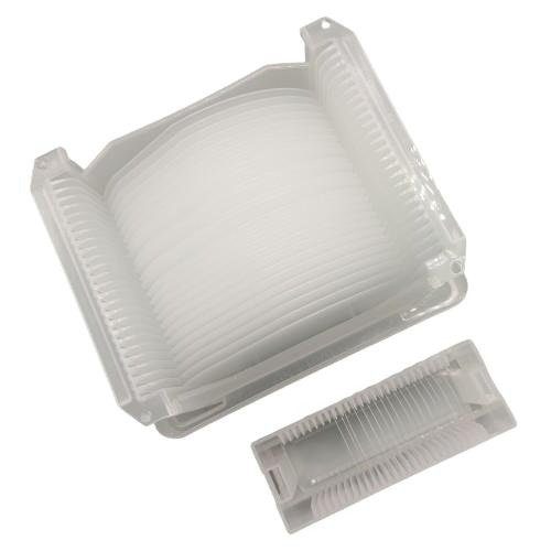
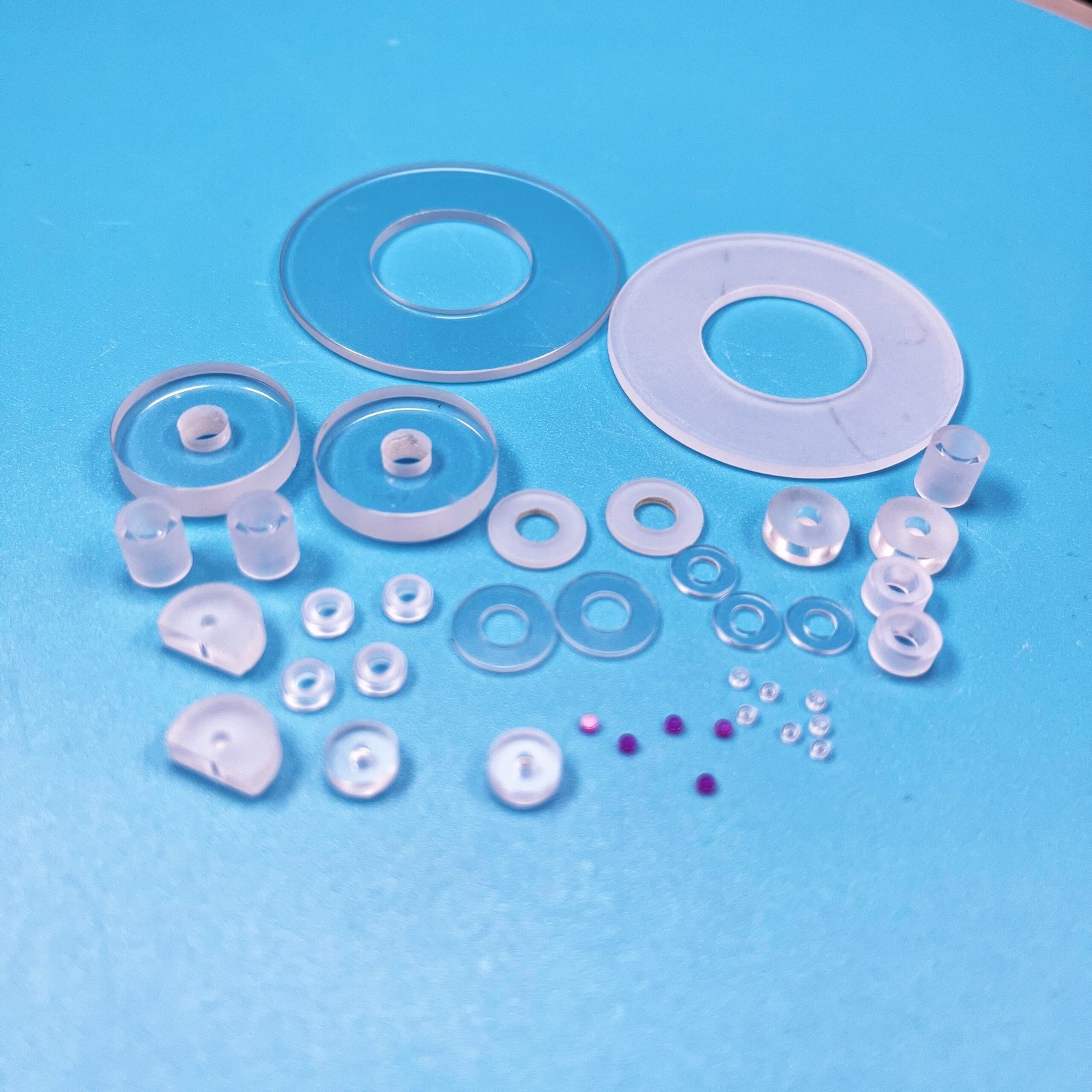
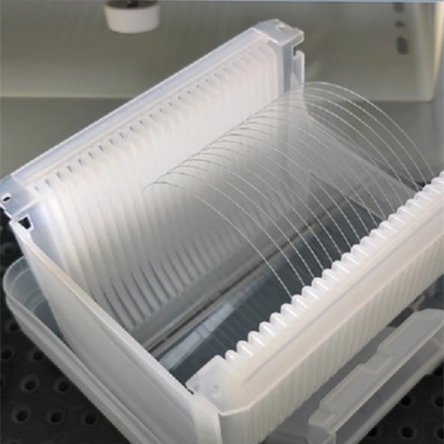
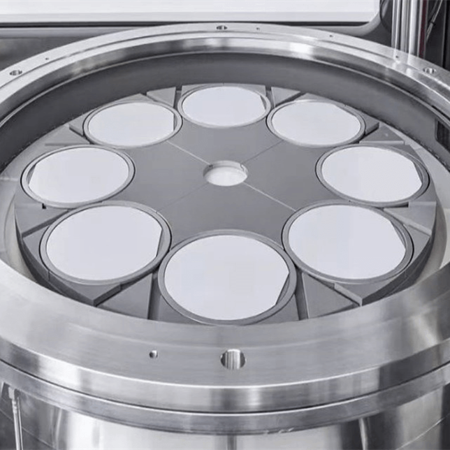
Crystal growers create sapphire ingots using Kyropoulos or Czochralski methods. You cut, grind, and polish wafers until they reach target dimensions. Through chemical-mechanical polishing (CMP), you receive epi-ready surfaces with sub-nanometer roughness.
You request custom flats, miscut angles, or drilled vias. You also choose SSP or DSP depending on whether you need one or both sides polished. By tailoring specifications, you adapt sapphire wafer precisely to your device.
Why Sapphire Wafer Outperforms Alternatives
You compare sapphire with silicon, SiC, and quartz. Silicon lacks thermal stability and optical transmission. SiC delivers conductivity but costs more, and it lacks transparency. Quartz transmits light but fails in hardness and dielectric strength. Only sapphire wafer provides the balance of durability, clarity, and high-temperature reliability.
You exploit these advantages, so you secure yield improvements and long-term performance in LEDs, lasers, RFICs, and sensors.
Q&A: Sapphire Wafer
Q: Why use 500 µm thickness for sapphire wafer?
A: You gain mechanical durability while keeping process compatibility.
Q: What is the key difference between 4-inch and 6-inch sapphire wafer?
A: You apply 4-inch for flexible research and you use 6-inch for high-volume manufacturing.
Q: Can sapphire wafer handle > 1000 °C processing?
A: Yes, sapphire remains dimensionally stable even under extreme heat.
Q: How does polishing type affect sapphire wafer?
A: You select SSP if one side needs epi-ready polish, and DSP if both sides must remain polished.
Q: Is customization available?
A: Absolutely, you specify orientation, bevel, miscut, or surface patterns according to device needs.
