

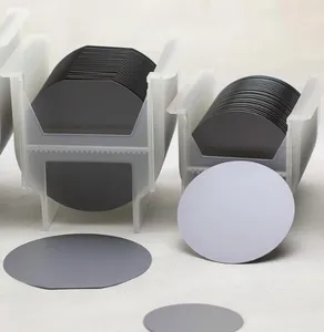
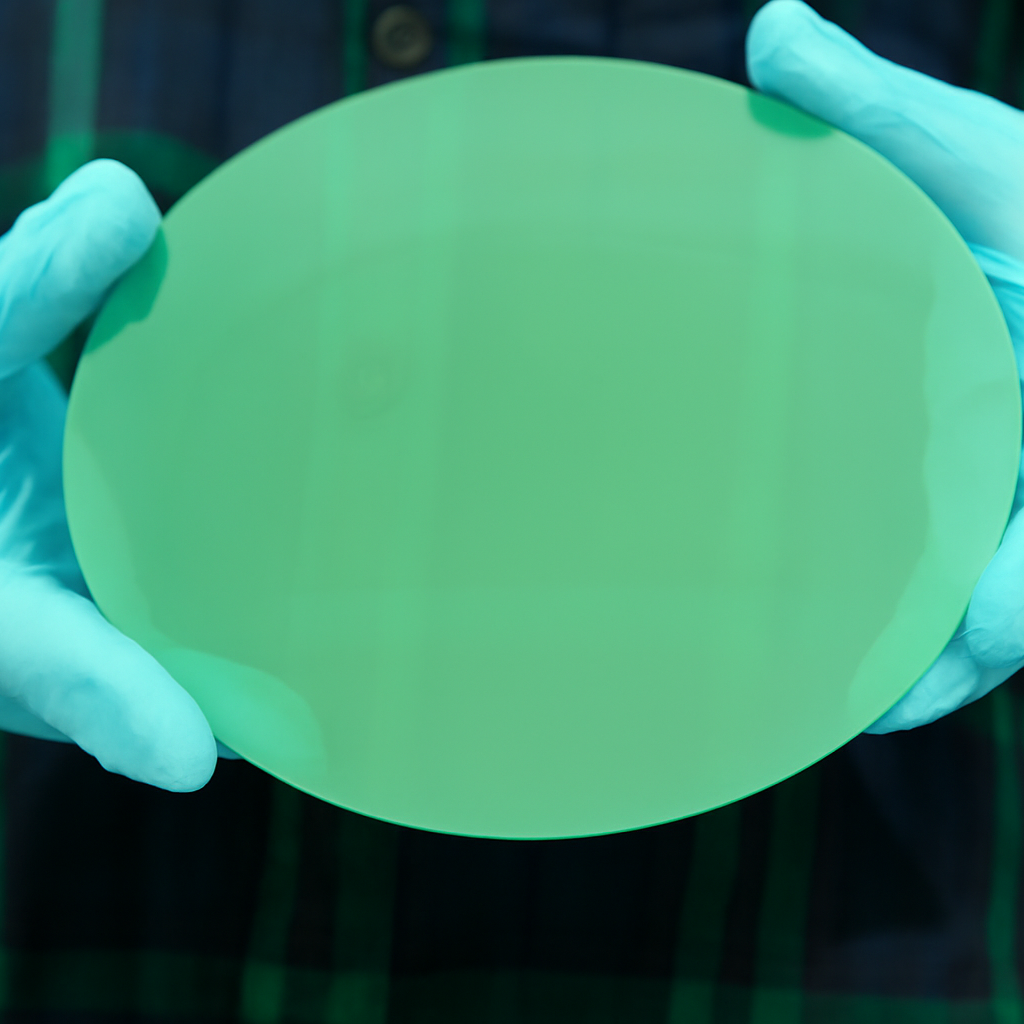
Product Information – Sapphire Wafer
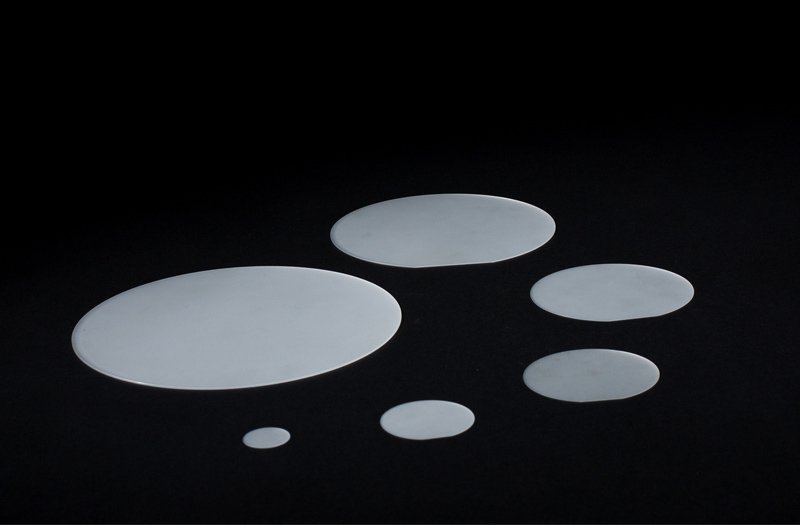
Product Name: Sapphire Wafer (2″ / 4″ / 6″ / 8″ / 12″)
Material: High-purity single crystal sapphire (Al₂O₃)
Crystal Structure: Hexagonal, single crystal, defect-free
1. Product Overview
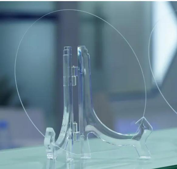
Sapphire wafers are high-performance single crystal substrates widely used in the semiconductor, optoelectronics, and optical industries. Thanks to their exceptional mechanical strength, high thermal conductivity, and outstanding chemical stability, sapphire wafers are the preferred material for applications that demand extreme durability, precision, and purity.
We offer sapphire wafers in a variety of diameters, including 2 inch, 4 inch, 6 inch, 8 inch, and 12 inch, with customization options for thickness, surface finish, and orientation to meet your specific application needs.
2. Technical Specifications
| Diameter | Size (mm) | Thickness (mm) | Orientation | Surface Finish | TTV (µm) | Ra (nm) |
|---|---|---|---|---|---|---|
| 2″ | 50.8 ± 0.1 | 0.3–1.0 | C-plane / A-plane / R-plane | SSP / DSP | ≤ 5 | ≤ 0.5 |
| 4″ | 100 ± 0.2 | 0.4–1.2 | C-plane / A-plane / R-plane | SSP / DSP | ≤ 5 | ≤ 0.5 |
| 6″ | 150 ± 0.3 | 0.5–1.5 | C-plane / A-plane / R-plane | SSP / DSP | ≤ 5 | ≤ 0.5 |
| 8″ | 200 ± 0.5 | 0.6–2.0 | C-plane / A-plane / R-plane | SSP / DSP | ≤ 5 | ≤ 0.5 |
| 12″ | 300 ± 0.5 | 0.8–3.0 | C-plane / A-plane / R-plane | SSP / DSP | ≤ 5 | ≤ 0.5 |
3. Key Features & Advantages
Extreme Hardness: Mohs hardness of 9, second only to diamond, ensuring excellent wear resistance.
High Temperature Resistance: Stable performance up to 2000°C in vacuum or inert atmosphere.
Optical Excellence: High transparency from UV (200 nm) to IR (5 μm) range.
High Dielectric Strength: Ideal for high-frequency and high-power electronic applications.
Chemical Resistance: Unaffected by most acids and alkalis, ensuring durability in harsh environments.
Precision Surface: Ultra-low surface roughness (Ra ≤ 0.5 nm) suitable for epitaxy growth.
4. Applications
LED Industry: As substrates for GaN, Al₂O₃, and InGaN epitaxial growth in blue, green, and white LEDs.
Semiconductors: Used in RFIC, power devices, and high-frequency ICs.
Optical Devices: Windows, lenses, and covers for high-power lasers, optical instruments, and cameras.
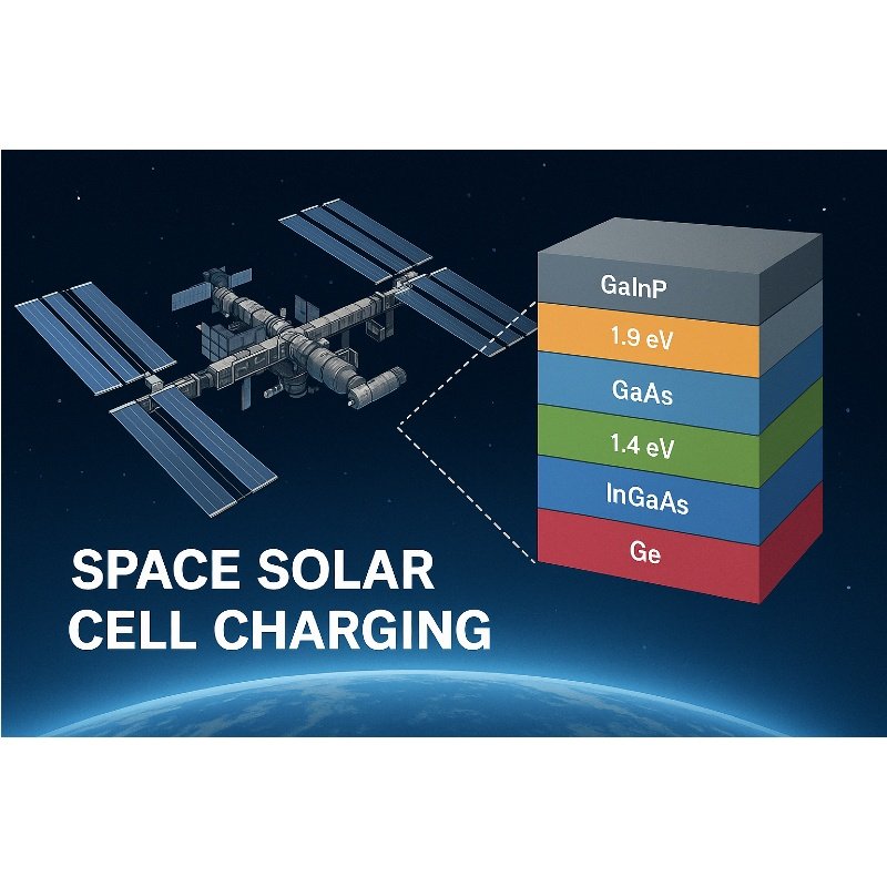
Scientific Research: Substrates for microfabrication, MEMS devices, and quantum technology.
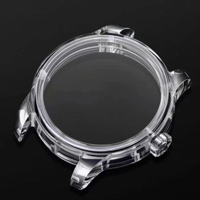
Luxury Goods: High-end watch crystals, precision instruments, and decorative applications.
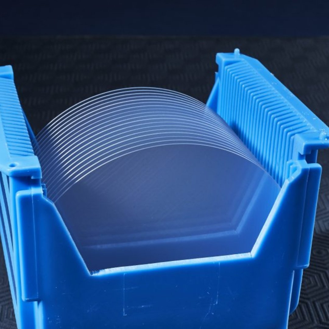
5. Packaging & Delivery
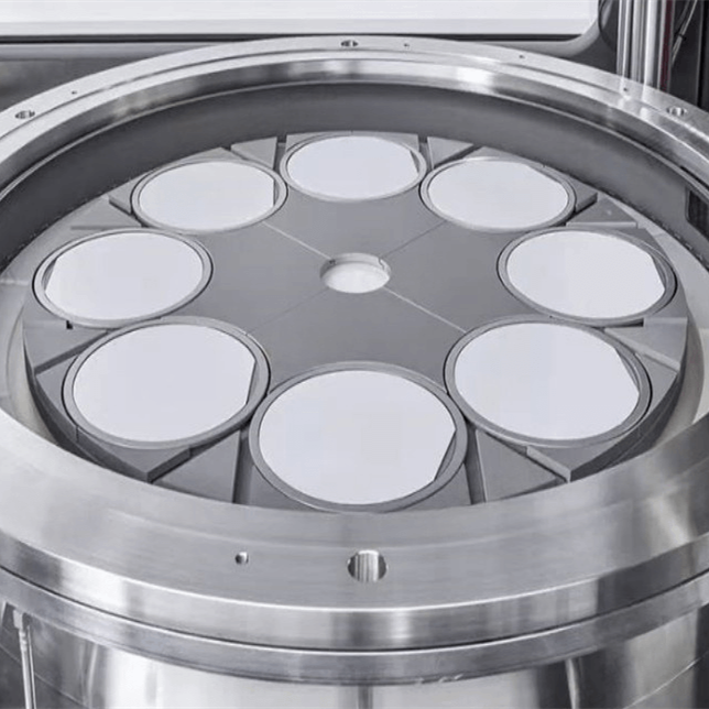
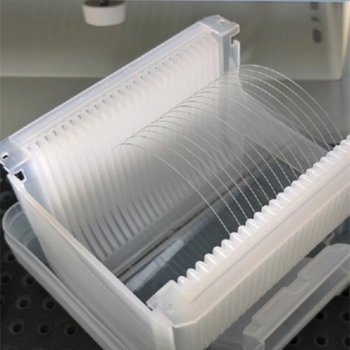
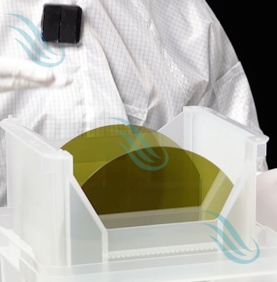
Packed in Class 100 cleanroom environment.
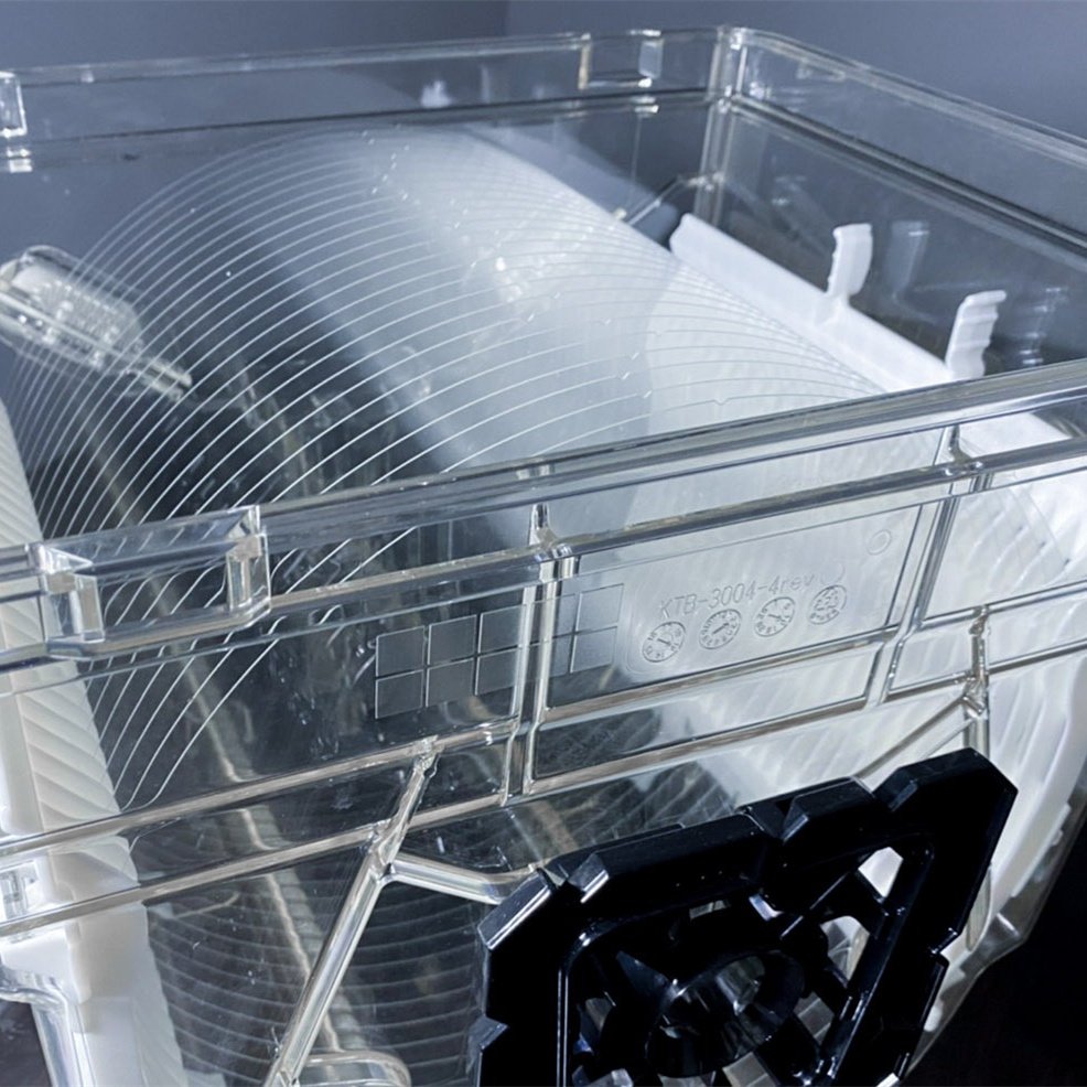
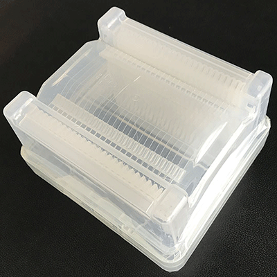
Each wafer is placed in a single wafer container or wafer cassette.
Vacuum sealed and shipped with shock–proof protective packaging.
Global shipping with express delivery options (DHL, FedEx, UPS).
6. Customization Options
Diameter: 2″, 4″, 6″, 8″, 12″ or customized size.
Thickness: From 0.2 mm to 5 mm depending on diameter.
Orientation: C-plane (0001), A-plane (11-20), R-plane (1-102), others on request.
Polishing: Single side polished (SSP), double side polished (DSP), or as-cut.
Flat / Notch: SEMI standard or customized.