

Sapphire Wafer 2 Inch, 4 Inch, 6 Inch, 8 Inch, and 12 Inch – Advanced Substrate for Semiconductor and Optoelectronics
Introduction
The demand for high-quality substrates keeps increasing because industries such as LED, RF, laser optics, and semiconductor devices continue to expand. Traditional substrates cannot always deliver the required thermal stability, surface quality, and mechanical strength. Therefore, many global manufacturers choose sapphire wafer as the foundation for advanced devices.
Artificial sapphire (Al₂O₃ ≥ 99.99%) combines exceptional hardness, excellent thermal conductivity, and outstanding optical transparency. Because of these unique properties, sapphire wafers from 2 inch to 12 inch sizes remain essential for epitaxial growth, power electronics, and photonic applications.
Product Overview
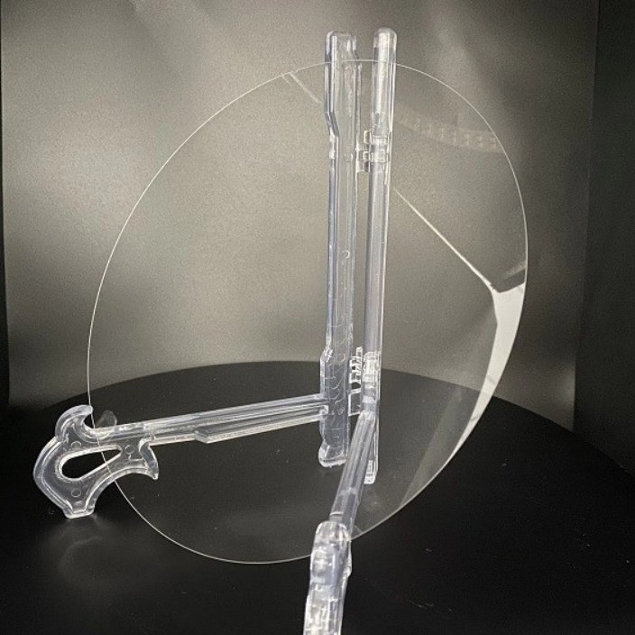
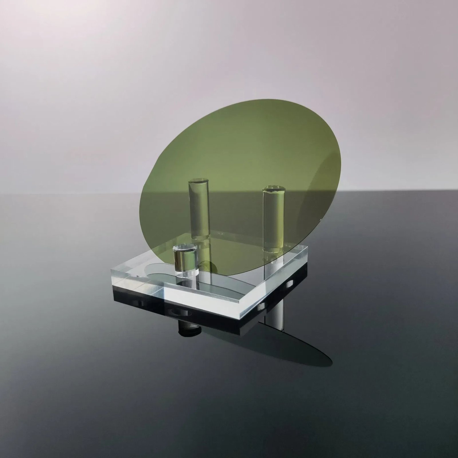
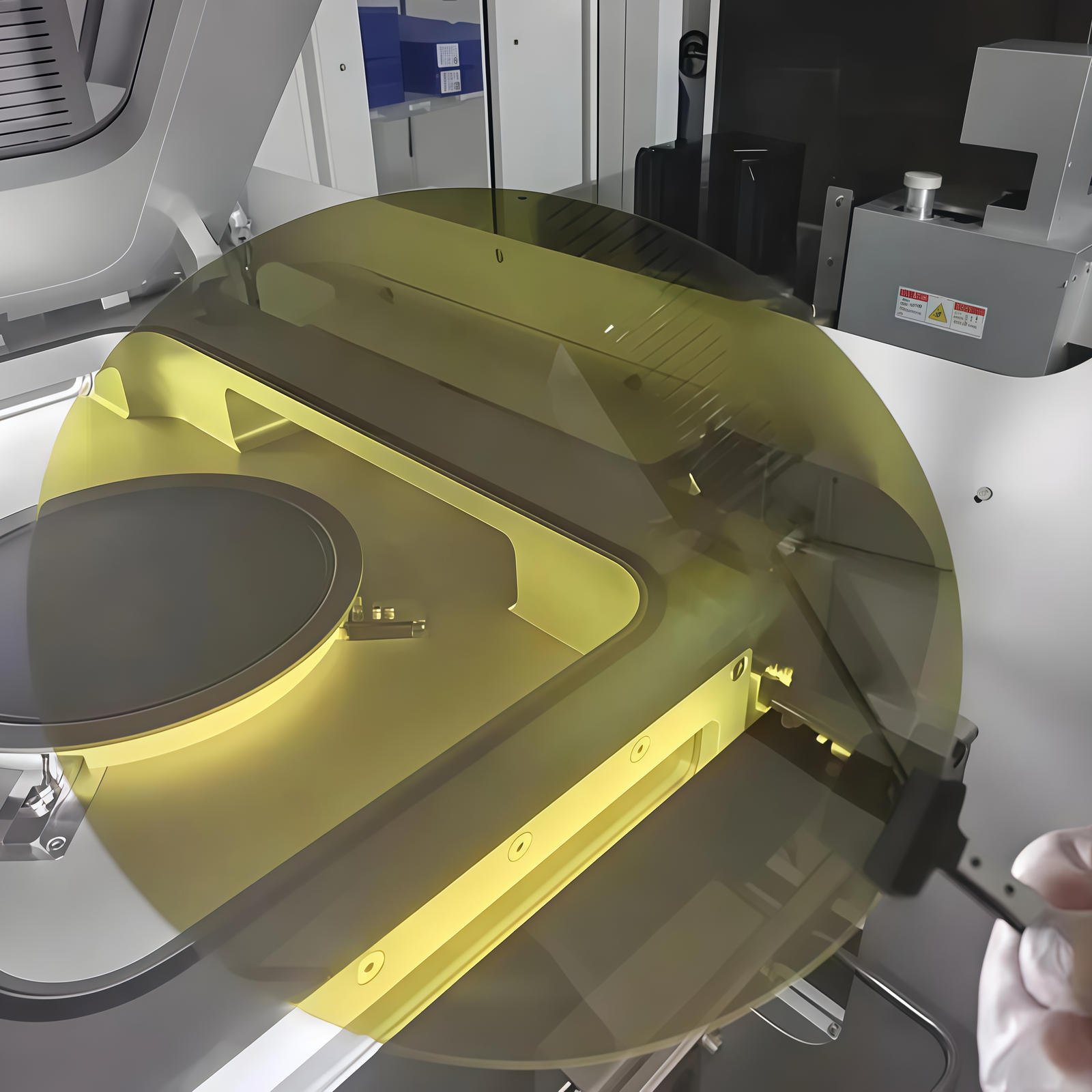
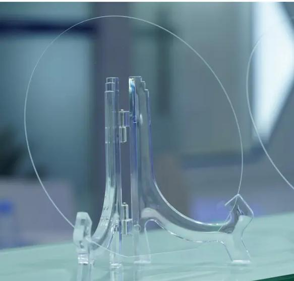
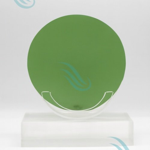
We provide sapphire wafer products in 2, 4, 6, 8, and 12 inch diameters. Each wafer follows strict quality standards to guarantee stable performance and reproducibility. With c-plane (0001) orientation and epi-ready finishing, these wafers support GaN-on-sapphire growth, laser diodes, and optical devices.
Moreover, our wafers pass advanced cleaning and inspection to meet Prime Grade requirements, ensuring low particle density, low metal contamination, and high reliability for mass production.
Technical Specifications
The table below summarizes the main specifications of our sapphire wafers:
| Item | 2 inch | 4 inch | 6 inch | 8 inch | 12 inch |
|---|---|---|---|---|---|
| Diameter | φ2 inch | φ4 inch | φ6 inch | φ8 inch | φ12 inch |
| Material | Artificial sapphire (Al₂O₃ ≥ 99.99%) | Same | Same | Same | Same |
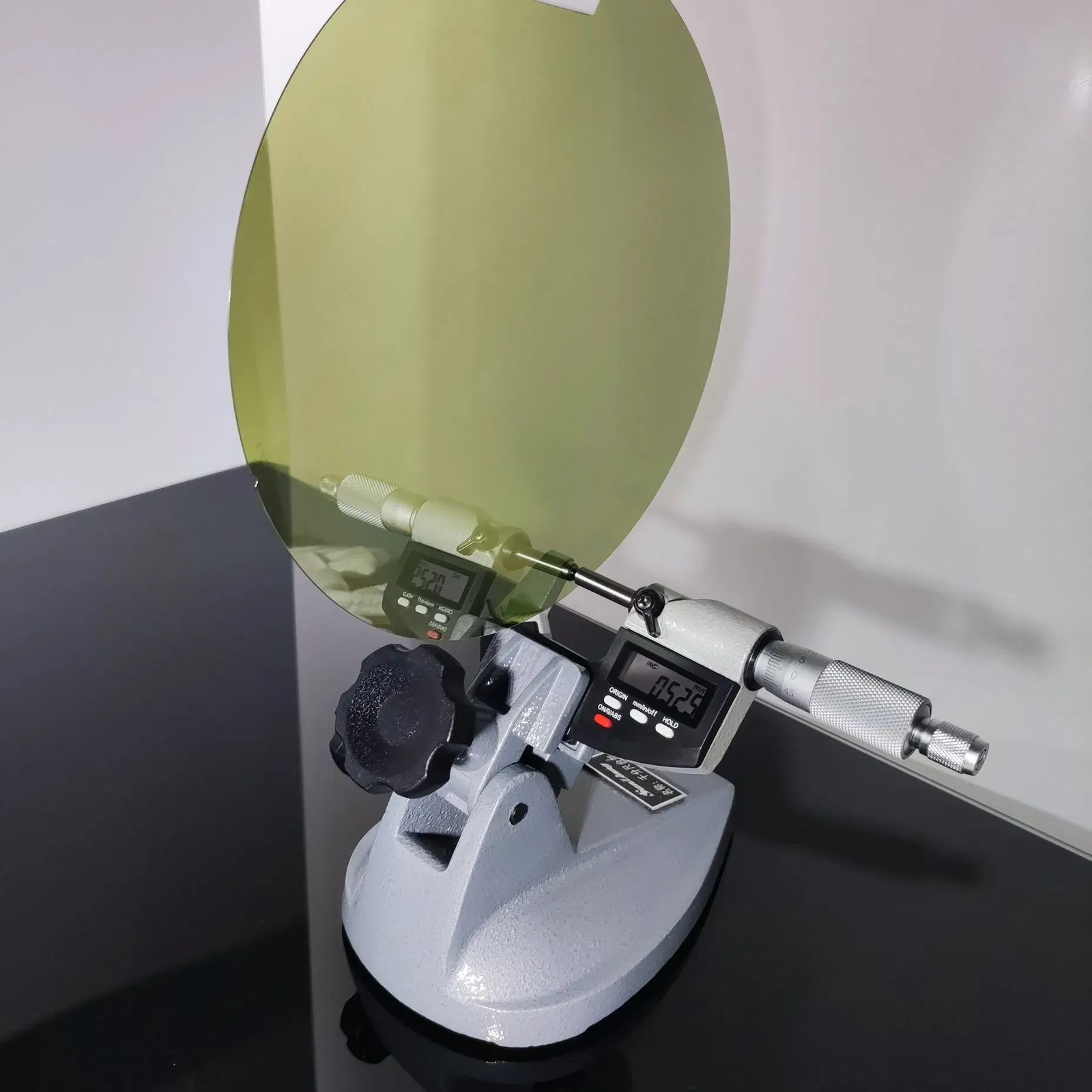
| Thickness | 430 ± 15 μm | 650 ± 15 μm | 1300 ± 20 μm | 1300 ± 20 μm | 3000 ± 20 μm |
| Surface orientation | c-plane (0001) | c-plane (0001) | c-plane (0001) | c-plane (0001) | c-plane (0001) |
| OF length | 16 ± 1 mm | 30 ± 1 mm | 47.5 ± 2.5 mm | 47.5 ± 2.5 mm | Negotiable |
| OF orientation | a-plane 0 ± 0.3° | a-plane 0 ± 0.3° | a-plane 0 ± 0.3° | a-plane 0 ± 0.3° | a-plane 0 ± 0.3° |
| TTV | ≤ 10 μm | ≤ 10 μm | ≤ 15 μm | ≤ 15 μm | Negotiable |
| BOW | -10 ~ 0 μm | -15 ~ 0 μm | -20 ~ 0 μm | -25 ~ 0 μm | Negotiable |
| Warp | ≤ 15 μm | ≤ 20 μm | ≤ 25 μm | ≤ 30 μm | Negotiable |
| Front side finishing | Epi-ready (Ra < 0.3 nm) | Same | Same | Same | Same |
| Back side finishing | Lapping (Ra 0.6 – 1.2 μm) | Same | Same | Same | Same |
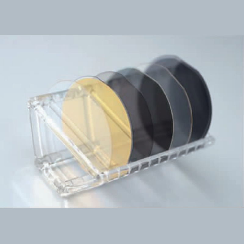
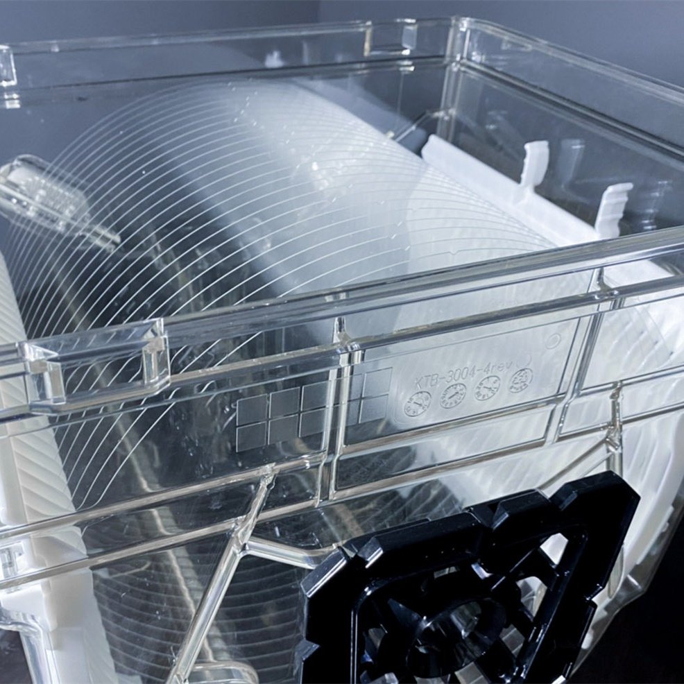
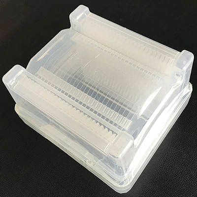
| Packaging | Vacuum packaging in clean room | Same | Same | Same | Same |
| Prime grade | Particles ≥ 0.3 μm ≤ 0.18 pcs/cm², metal contamination ≤ 2E10/cm² | Same | Same | Same | Same |
Grade and Quality
We offer Prime Grade sapphire wafer with high-quality cleaning. Because particle density and metal contamination remain strictly controlled, the wafers meet advanced epitaxy requirements.
Particles: ≥ 0.3 μm, ≤ 0.18 pcs/cm².
Metal contamination: ≤ 2E10/cm².
Flatness and uniformity: Controlled TTV, BOW, and Warp.
These parameters ensure stable epitaxial growth for GaN, AlN, and related compound semiconductors.
Advantages of Our Sapphire Wafers
Choosing our sapphire wafer provides several benefits:
Wide Range of Sizes: 2, 4, 6, 8, and 12 inch diameters cover R&D, pilot, and mass production.
Epi-Ready Surface: Ultra-smooth Ra < 0.3 nm guarantees superior epitaxial growth.
Mechanical Strength: Thickness up to 3000 μm ensures durability during processing.
Thermal Stability: Al₂O₃ offers excellent thermal conductivity and stability under extreme conditions.
Optical Transparency: C-plane orientation supports optical and laser applications.
Strict Cleanroom Packaging: Vacuum-sealed wafers arrive contamination-free.
Because of these features, customers gain consistent results and reduced production costs.
Applications
The use of sapphire wafer spans across multiple industries:
LED Manufacturing: GaN-on-sapphire epitaxy supports blue and white LEDs.
RF and Power Devices: Stable substrates for GaN HEMTs and RF amplifiers.
Laser Diodes: High-quality surfaces improve optical performance.
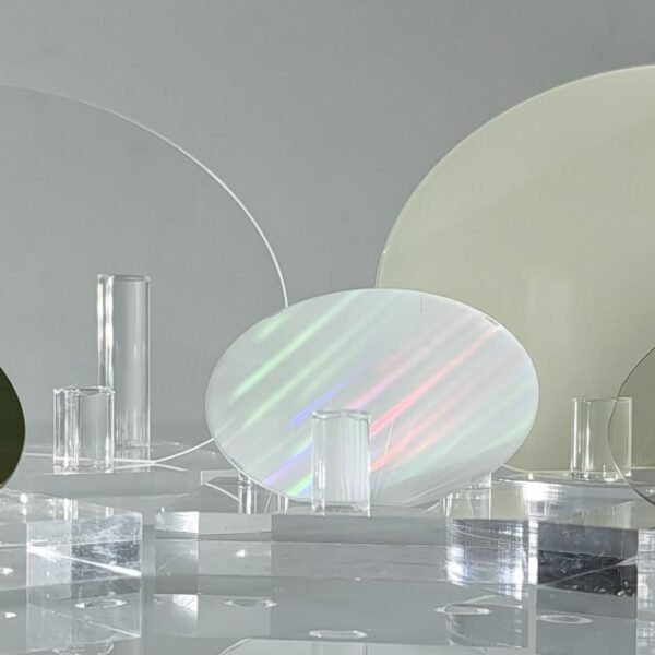
Optical Windows: Transparent sapphire supports high-intensity optical systems.
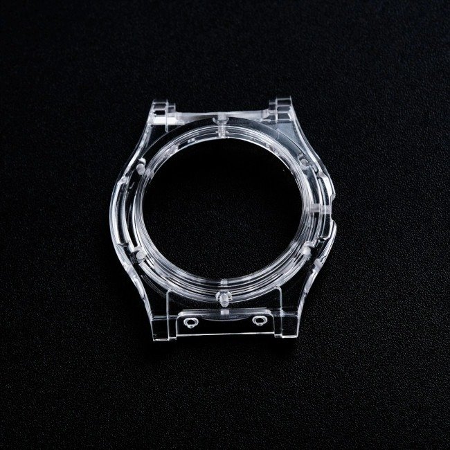
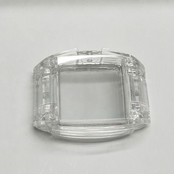
Watch and Consumer Electronics: Durable sapphire substrates provide scratch resistance.
Research and Development: 2 inch and 4 inch wafers serve universities and labs.
Therefore, whether for mass production or academic research, our sapphire wafers deliver unmatched performance.
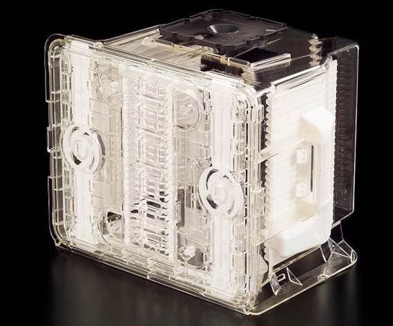
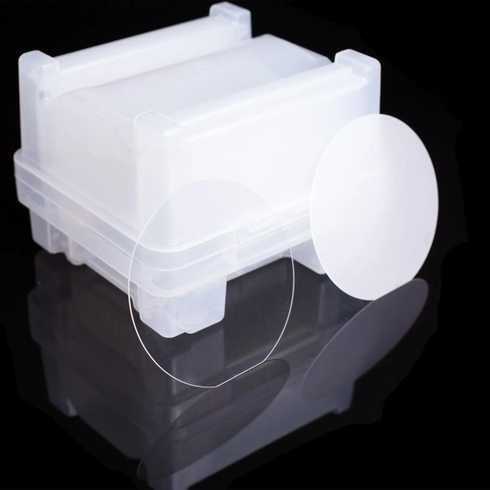
Packaging and Delivery
Every sapphire wafer receives vacuum packaging inside a cleanroom environment. Multi-wafer cassettes or single-wafer containers protect the wafers during storage and transport. Because safe handling matters, we ensure secure delivery to customers worldwide.
Conclusion and Call to Action
The sapphire wafer in 2, 4, 6, 8, and 12 inch diameters represents the best choice for semiconductor, LED, and optical applications. With Al₂O₃ ≥ 99.99%, epi-ready finishing, and strict Prime Grade standards, our wafers provide reliable performance for research and industry.
If you need sapphire wafer solutions, contact our sales team today. We provide fast quotations, technical support, and secure global shipping. Because your success depends on stable materials, we dedicate ourselves to delivering wafers that help you innovate and lead your market.