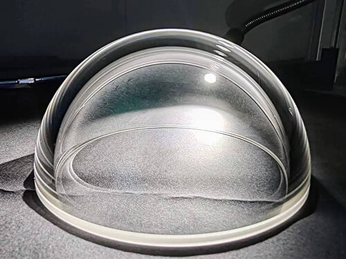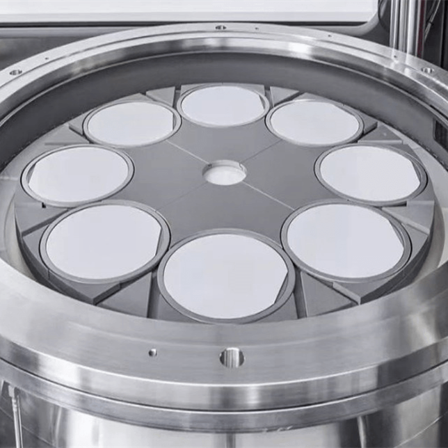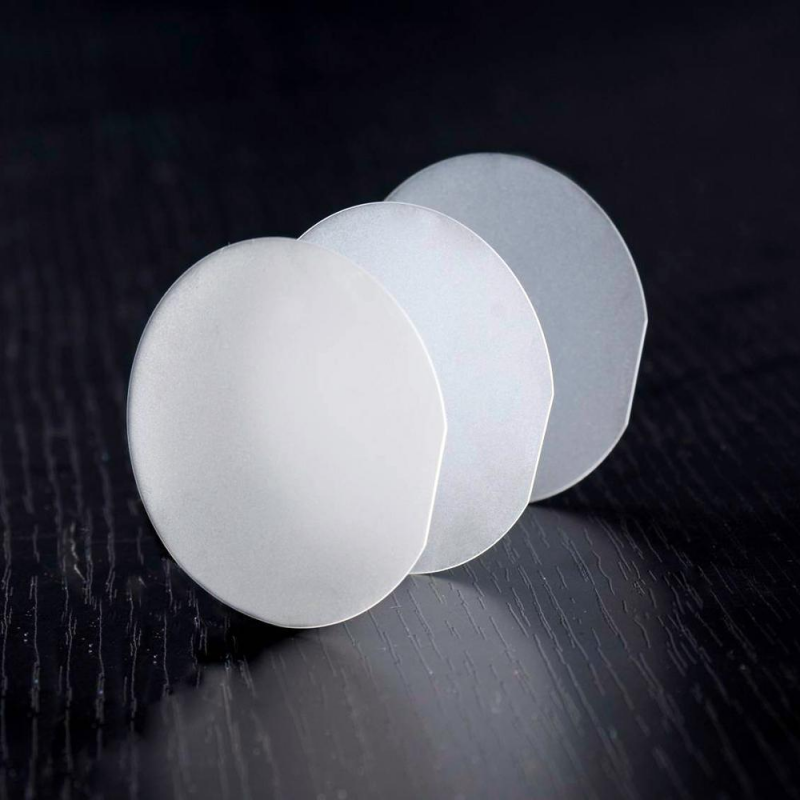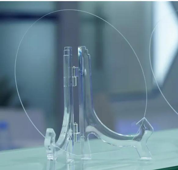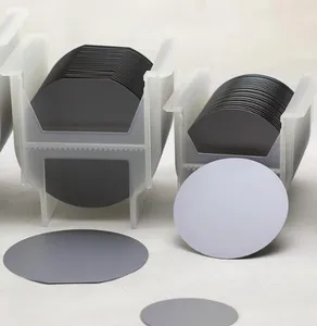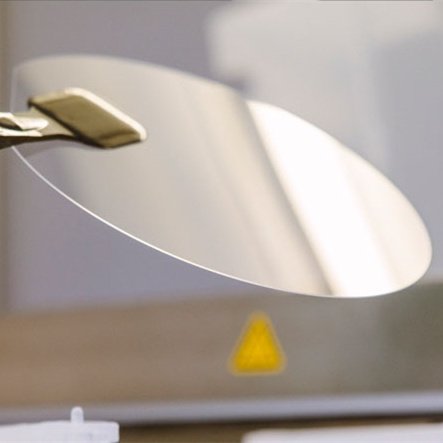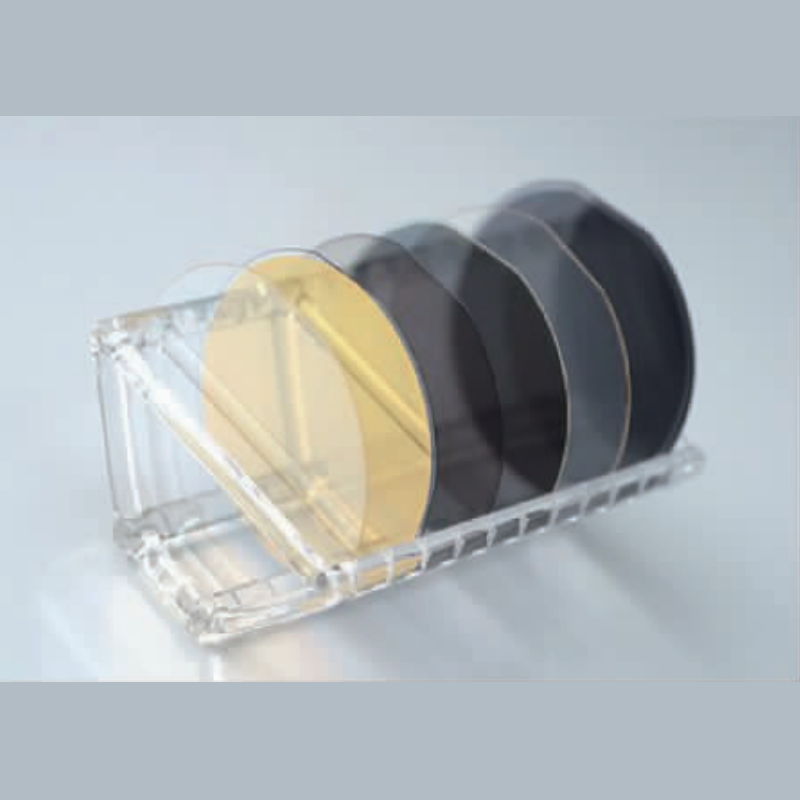

12-Inch Sapphire Wafer (Al₂O₃, 775 µm) – Advanced Substrate for Industrial Applications
The sapphire wafer in 12-inch (300 mm) diameter and 775 µm thickness represents the frontier of large-scale semiconductor substrates. When you adopt this sapphire wafer, you gain unmatched crystalline stability, excellent optical transparency, high thermal endurance, and mechanical hardness. Because sapphire substrate delivers all these properties in a 12-inch size, you advance into true mass-production territory for LEDs, lasers, RFICs, and emerging photonic devices.
You benefit from scaling up without compromising quality. You also achieve higher yields across larger areas, and you reduce cost per unit at volume. Moreover, you leverage sapphire wafer’s ability to transmit across UV to IR, while maintaining Mohs hardness of 9 and chemical inertness. Thus, the 12-inch sapphire substrate gives you the power to align with next-generation device requirements.
Why Choose the 12-Inch Sapphire Wafer
You obtain maximum throughput with the 12-inch sapphire wafer, because it offers nearly four times the usable area of a 6-inch wafer. You also optimize cost per die while preserving superior flatness and low defect density.
You rely on its ≥ 99.999% purity Al₂O₃, so you secure defect-controlled epitaxy for GaN and other III-V compounds. You also take advantage of sub-nanometer epi-ready surfaces that boost yields. Additionally, sapphire wafer tolerates > 1000 °C processing, and you can integrate it into high-frequency devices with confidence.
You benefit not only in performance but also in standardization. Industry leaders now regard the 12-inch sapphire wafer as the ultimate format for scaling LED production, silicon-on-sapphire circuits, and advanced laser devices.
Key Features of Sapphire Wafer
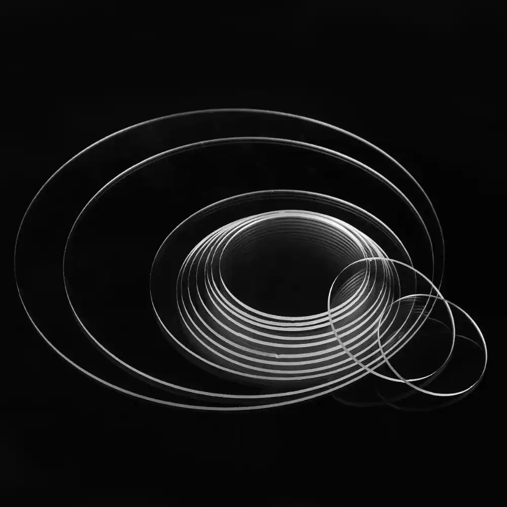
Large 300 mm diameter ensures scalability in industrial production lines.
775 µm thickness supports mechanical strength and processing compatibility.
Epi-ready polish Ra < 0.2 nm secures defect-free epitaxy.
High purity ≥ 99.999% Al₂O₃ provides excellent crystal uniformity.
Thermal reliability > 1000 °C enables demanding processes.
Optical transparency 200 nm–5 µm covers UV, visible, and IR.
Dielectric strength ~4.8×10⁵ V/cm ensures insulation for RF and SOS devices.
Mohs hardness 9 guarantees durability against scratching and abrasion.
Technical Specifications of 12-Inch Sapphire Wafer
| Parameter | Specification (Typical) |
|---|---|
| Material Purity | ≥ 99.999% Al₂O₃ single crystal |
| Diameter | 300 mm ± 0.2 mm (≈ 12 inch) |
| Thickness | 775 µm ± 20 µm |
| Orientation | C-plane (0001) standard; A-, R-, M-planes available |
| Surface Finish | SSP: epi-ready one side Ra < 0.2 nm; DSP: both sides polished Ra < 0.2 nm |
| TTV / Bow / Warp | ≤ 30 µm |
| Primary Flat & Length | A-plane primary flat ≈ 57.5 mm ± 2 mm |
| Edge Profile | SEMI standard bevel or customized |
| Thermal Expansion Coefficient | ∥ C-axis: 6.66×10⁻⁶ /°C; ⟂ C-axis: 5.0×10⁻⁶ /°C |
| Thermal Conductivity | 30–42 W/(m·K) at 25 °C |
| Dielectric Constant | ∥ C-axis ≈ 11.5; ⟂ C-axis ≈ 9.3 |
| Dielectric Strength | ~4.8×10⁵ V/cm |
| Refractive Index | ~1.77 (visible spectrum) |
| Optical Transmission | 200 nm – 5 µm |
| Mohs Hardness | 9 |
Applications of 12-Inch Sapphire Substrate
1. LED and GaN Epitaxy
You deploy 12-inch sapphire wafers in LED production lines, because you achieve high yields for GaN epitaxy. You cut costs per chip, and you sustain growth in blue, green, and UV LEDs.
2. Laser and Photonic Devices
You use sapphire substrate in UV lasers, IR detectors, and photonic filters. Its broad spectrum transparency enables reliable optical output.
3. RFIC and Silicon-on-Sapphire Devices
You rely on sapphire wafer for RFIC and SOS circuits, because its dielectric strength reduces loss and ensures insulation.
4. Optical Windows and Instrumentation
You fabricate large optical windows, precision lenses, and scientific instruments from 12-inch sapphire substrate. Its hardness and chemical resistance extend durability.
5. Research and Pilot Lines
You support advanced research at scale, because the 12-inch sapphire wafer bridges laboratory development and industrial production.
Manufacturing and Customization
Crystal growers use Kyropoulos (KY) or Czochralski (CZ) techniques to produce 12-inch sapphire boules. After cutting, wafers undergo grinding, lapping, and polishing. Because manufacturers apply chemical-mechanical polishing (CMP), surfaces reach epi-ready Ra < 0.2 nm.
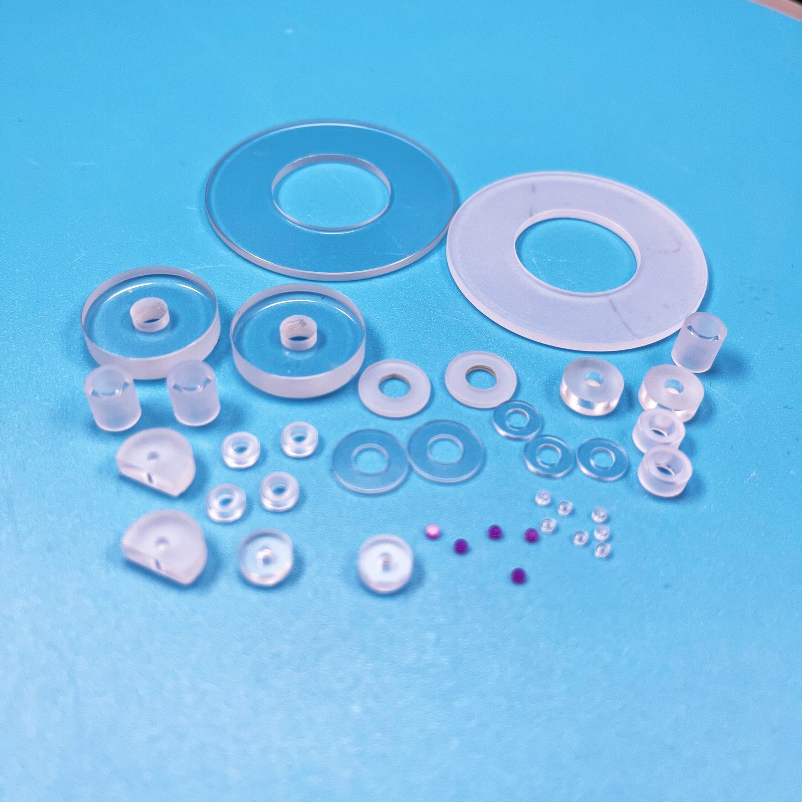
You customize wafers with flats, miscut angles, or drilled vias. You also order different orientations or thicknesses, depending on device requirements. This flexibility ensures that sapphire wafer aligns perfectly with your application.
Why Sapphire Wafer Surpasses Alternatives
You compare sapphire wafer with silicon, SiC, or quartz. Silicon lacks thermal stability and optical transparency. SiC offers conductivity but costs more and lacks UV–IR clarity. Quartz is transparent but cannot match sapphire’s hardness and dielectric properties. Therefore, you rely on sapphire wafer, because it combines durability, cost-effectiveness, optical clarity, and electrical insulation in one solution.
Q&A: About Sapphire Wafer
Q: Why is the 12-inch sapphire wafer significant for industry?
A: You scale production, reduce cost per die, and align with high-volume LED and RFIC demands.
Q: How does thickness (775 µm) influence performance?
A: You benefit from mechanical strength and process compatibility, while minimizing stress during epitaxy.
Q: Can sapphire wafer survive extreme heat?
A: Yes—you process devices at > 1000 °C, because sapphire wafer resists warping and thermal shock.
Q: How does sapphire compare with SiC?
A: You enjoy lower costs and optical transparency, while SiC mainly suits power electronics. Sapphire wafer dominates LEDs and photonics.
Q: Is customization possible for 12-inch sapphire substrate?
A: Absolutely—you order flats, off-angles, DSP polishing, or special surface features depending on application.