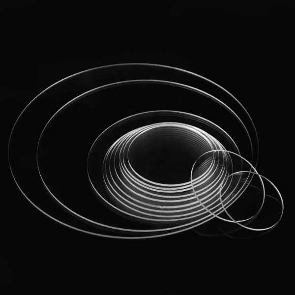

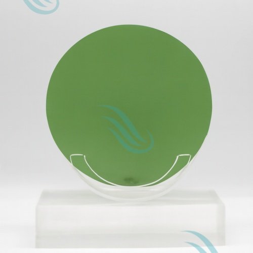
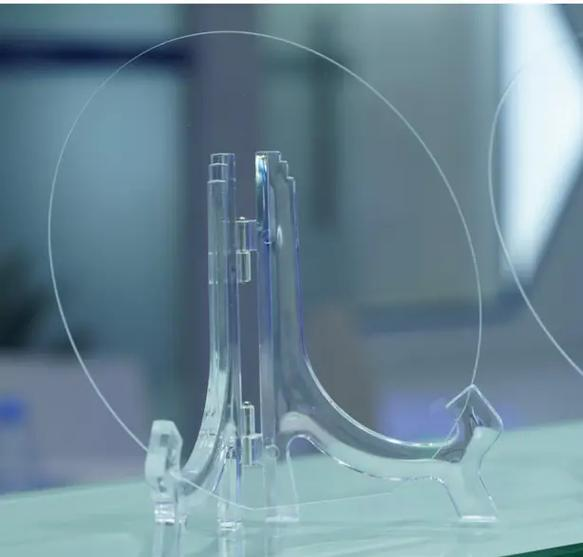
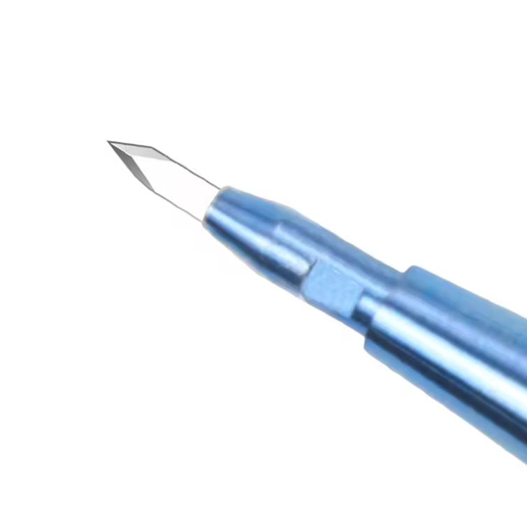
sapphire wafer 12inch 300mm Double side polish,single side polish
12-Inch Sapphire Wafer Product Description
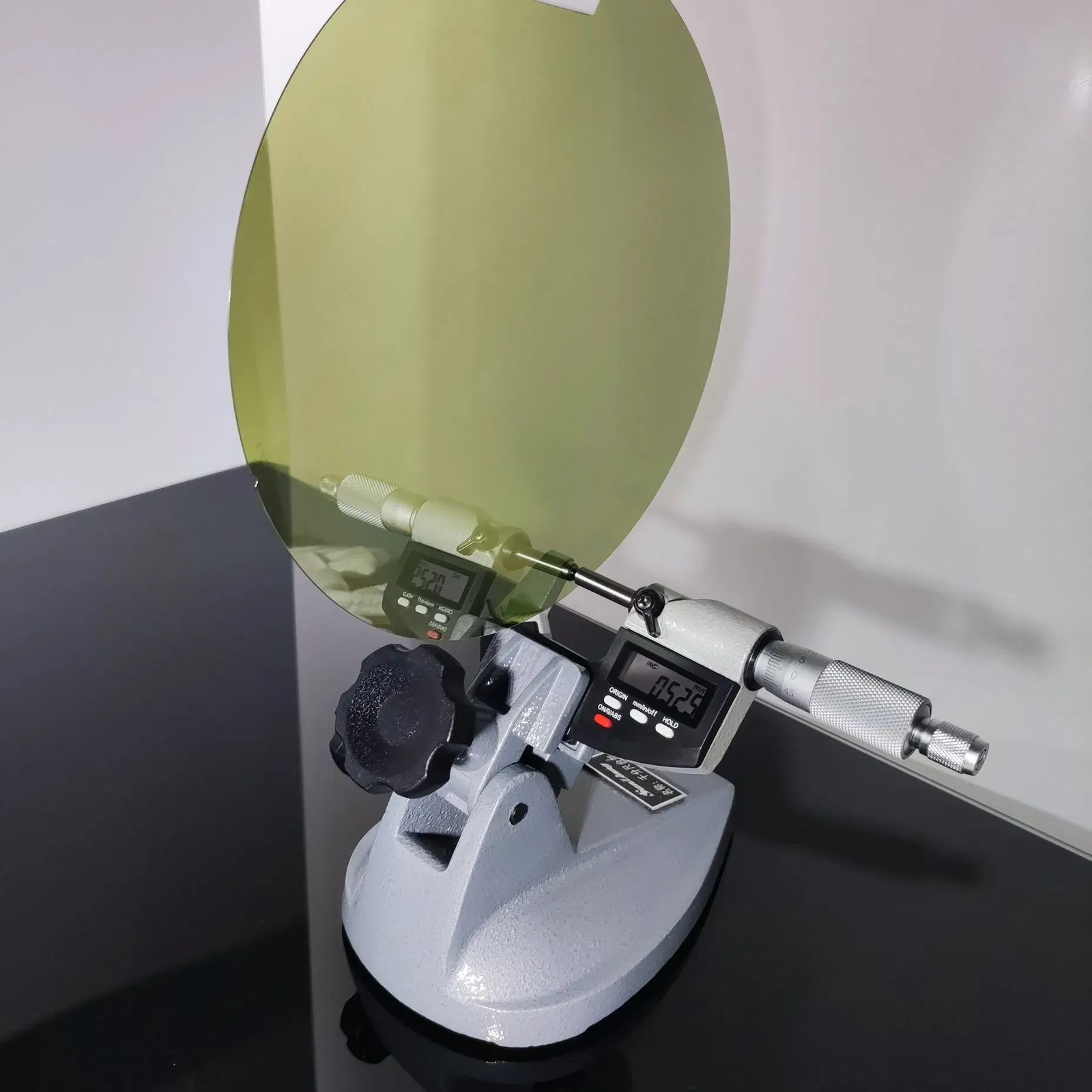
We manufacture our 12-inch sapphire wafers using the Kyropoulos (KY) method, which guarantees ultra-high purity (>99.999% Al2O3) and superior crystalline uniformity. The standard diameter is 300 ± 0.2 mm, and thickness options include 800 μm Moreover 1000 μm, and 1200 μm.
These wafers offer outstanding mechanical strength, excellent thermal conductivity, and long-term stability.
They serve as the ideal material for GaN-on-sapphire epitaxy, semiconductor device processing and micro-LED displays and and advanced optoelectronics.
The wafers feature a C-plane (0001) orientation with off-set angles of 0.0° ± 0.3° toward both the M-axis and A-axis Moreover ensuring precise alignment.
Each wafer includes an A-plane (0001) notch at 0° ± 1° orientation. The notch depth ranges from 1.0 to 1.25 mm, and the angle falls between 85° and 95°, which supports accurate lithography processes.
Additionally, the front surface comes epi-ready polished (Ra < 0.3 nm) and which optimizes GaN-on-sapphire deposition. The back surface is lapped (Ra 0.8–1.2 μm) and ensuring excellent stability during subsequent processing.
Bevels are crafted with T-type 200 ± 100 μm, which guarantees safety during handling and wafer durability.
We maintain strict quality standards. Our wafers achieve TTV ≤ 25 μm and BOW ≤ 35–40 μm, and WARP ≤ 120–150 μm.
We also limit scratches to ≤5 near the edge and ≤3 within the active area. We control bubble density and restrict chips to ≤0.2 mm² to ensure high-quality performance.
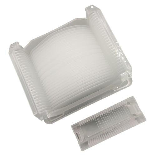
Finally, we deliver clean and residue-free, and individually packed wafers in CRC100 containers and protecting them during transport.
Why Choose Our Sapphire Wafers?
Enhanced Thermal Management: Sapphire’s superior thermal conductivity makes it ideal for high-power applications.
Durability: Sapphire’s hardness ensures long-lasting reliability in demanding environments.
Epi-Ready Surface: The Ra < 0.3 nm polished surface is perfect for epitaxial growth.
Industry Versatility: These wafers are widely used in LED manufacturing and semiconductor R&D, and 5G communication.
Our Manufacturing Process
Properties
Material: >99.999% High Purity Mono-crystalline Al2O3 (Kyropoulos method)
Diameter: 300 mm ± 0.2 mm
Thickness Options: 800 μm / 1000 μm / 1200 μm (±50 μm)
Orientation: C-Plane (0001), off-set toward M-axis/A-axis 0.0° ± 0.3°
Notch Orientation: A-Plane (0001) 0° ± 1°
wafer Notch Depth: 1.0–1.25 mm
Notch Angle: 85–95°
Front Surface: Epi-ready polished, Ra < 0.3 nm
Back Surface: Lapped, Ra 0.8 μm < Ra < 1.2 μm
Bevel: T-type, 200 μm ± 100 μm
Flatness: TTV ≤ 25 μm, BOW ≤ 35–40 μm, WARP ≤ 120–150 μm
Defect Control: ≤5 scratches near edge, ≤4 bubbles (10–60 μm), chips ≤0.2 mm²
Cleaning: No aggregation, no residue, particle-free
Packaging: CRC100 container, 1 pc/box
| 12inch sapphire wafer specification | |||
| Parameters | Production-1 | Production-2 | Production-3 |
| Material Sapphire | >99.999%, High Purity, Mono-crystalline Al2O3 (KY) | ||
| Diameter | 300mm±0.2mm | 300mm±0.2mm | 300mm±0.2mm |
| Thickness | 1000um±50um | 800um±50um | 1200um±50um |
| Orientation | C-Plane(0001)off-set | ||
| Off-set Angle toward M-axis | 0.0 ±0.3° | ||
| Off-set Angle toward A-axis | 0.0 ±0.3° | ||
| Notch Orientation | A-Plane(0001) 0°±1° | ||
| Notch Depth | 1.0-1.25mm | ||
| Notch Angle | 85-95° | ||
| Notch Chamfer | Customizable | ||
| Front Epi-ready polished | Ra < 0.3nm | ||
| Back Lapped or fine ground | 0.8um< Ra < 1.2um | 0.8um< Ra < 1.2um | 0.8um< Ra < 1.2um |
| Bevel | T-type 200um±100um | T-type 200um±100um | T-type 200um±100um |
| TTV | ≤25um | ≤25um | ≤25um |
| BOW | ≤35um | ≤40um | ≤35um |
| WARP | ≤120um | ≤150um | ≤120um |
| Scratch | 5 scratches allowed within 2mm of edge, 3 allowed beyond 2mm, length ≤3mm | ||
| Bubbles/Pits | ≤4 bubbles (10–60um) in effective area, distance >1mm; bubbles <10um not included; ≤60um in ineffective area | ||
| Chips | ≤0.2mm² | ||
| Cleaning | No aggregation or residue, particles not controlled | ||
| Laser mark | Customizable | ||
| Packing | CRC100 packed,1pc/box | ||
Applications
Our 12-inch sapphire wafers offer high versatility across a range of industries:
LED & Micro-LED Manufacturing: Sapphire wafers serve as the optimal substrate for GaN epitaxy and which ensures high brightness and long lifespan.
RF & Power Devices: They provide exceptional thermal insulation and electrical conductivity and making them ideal for high-frequency electronics.
Laser Diodes: Sapphire’s optical transparency and durability make it the perfect choice for blue and UV and high-power laser applications.
5G Communication: Sapphire wafers improve stability in high-frequency modules and which are crucial for 5G technologies.
Optical Windows & Lenses: These wafers offer exceptional clarity and strength and making them ideal for optical components.
Semiconductor R&D: Sapphire wafers are widely used in developing next-generation chips and advancing epitaxial technologies.
Q&A – Frequently Asked Questions
Q1: Why are sapphire wafers preferred over silicon for LED production?
A: Sapphire provides high thermal conductivity and chemical resistance, and mechanical strength and making it ideal for GaN-based LED growth.
These qualities result in better performance and longer lifespan compared to silicon.
Q2: Are the wafers ready for epitaxy?
A: Yes, the front surface is epi-ready polished (Ra < 0.3 nm) and which makes it perfectly suited for GaN-on-sapphire deposition.
Q3: What thickness options are available?
A: Our wafers come in standard thicknesses of 800 μm and 1000 μm, and 1200 μm. We can also provide custom thicknesses based on your specific needs.
Q4: How do you ensure quality?
A: We test every wafer for flatness and scratches and bubbles, and chips to ensure that they meet our rigorous quality standards.
Q5: What industries use 12-inch sapphire wafers?
A: These wafers are used in LED manufacturing and laser diodes and power electronics and RF ICs, optical windows, and 5G communication.