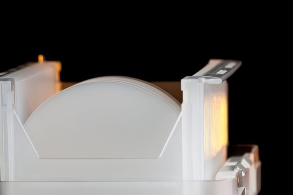

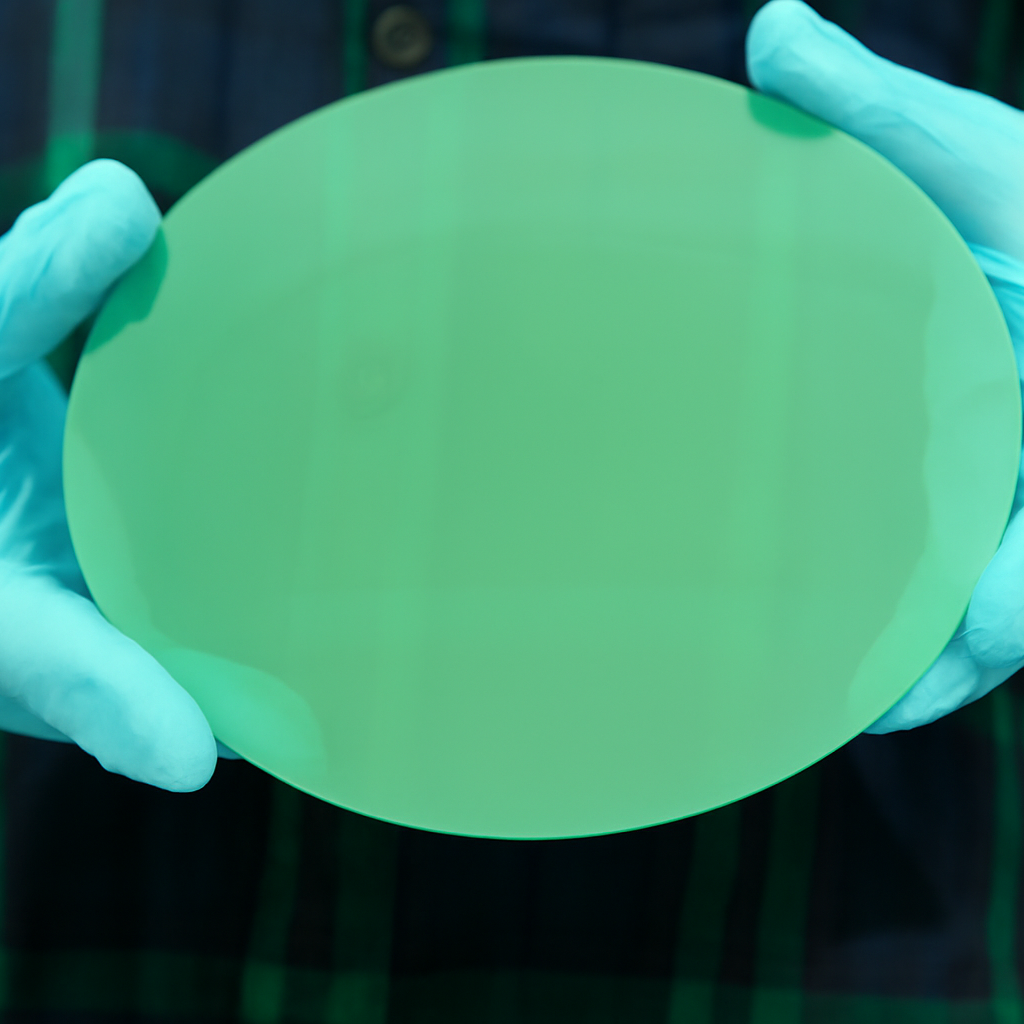
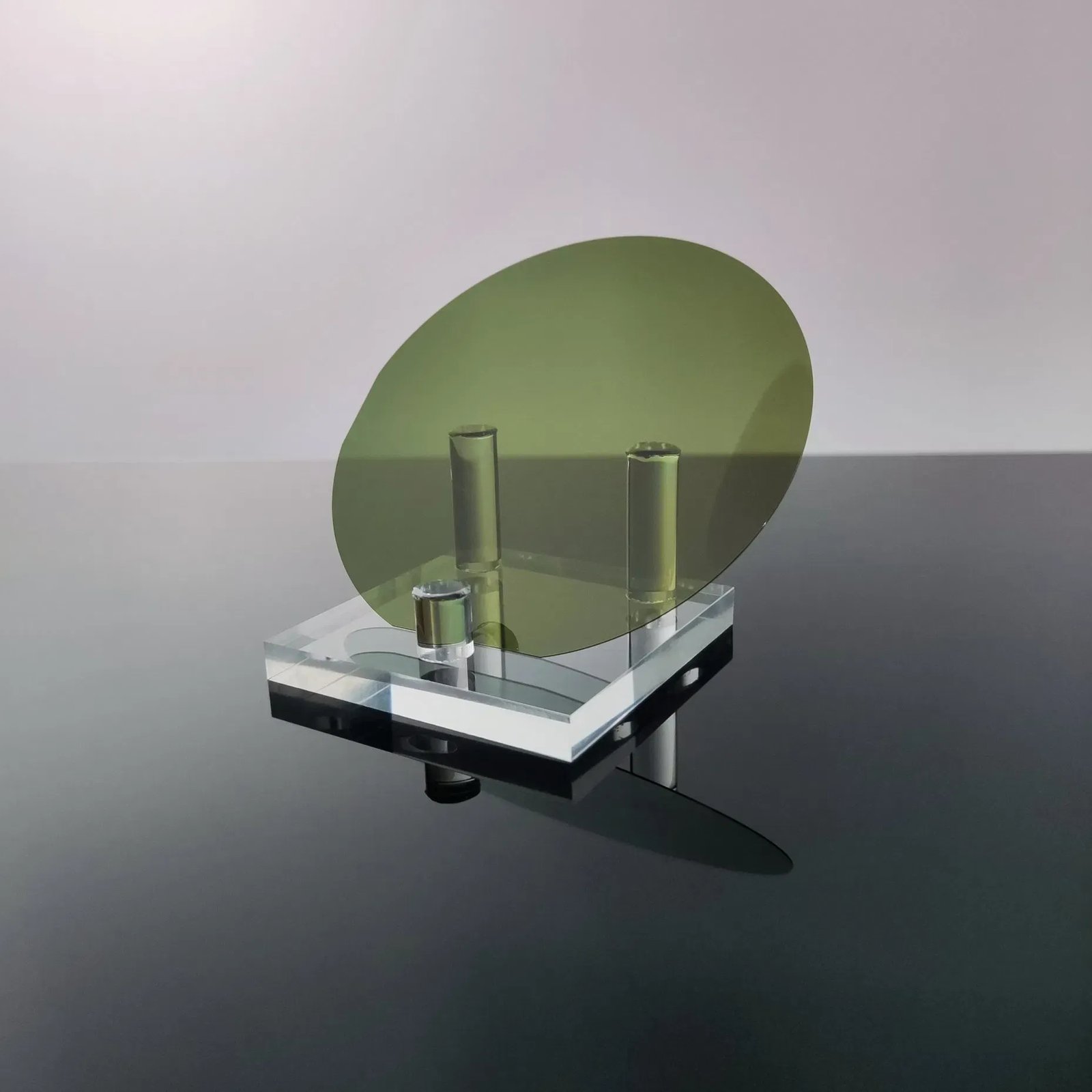
6-Inch Sapphire Substrate (Al₂O₃) – High-Performance Wafer for Optoelectronics and Semiconductors
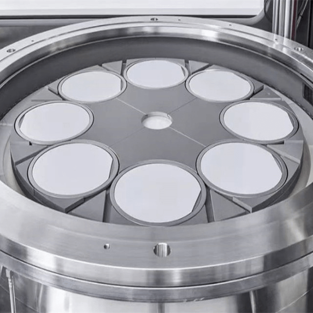
The sapphire substrate in 6-inch diameter represents the most widely adopted format for industrial-scale LED production and optoelectronic devices. When you choose a sapphire wafer, you gain a material that integrates thermal stability, optical transparency, mechanical hardness, and electrical insulation. Because sapphire substrate combines these features, it has become the backbone of mass production in advanced semiconductor and photonics industries.
You benefit from scalability, because 6-inch wafers increase throughput while reducing cost per device. You also maintain tight dimensional tolerances and high crystalline quality, so you improve epitaxial yields and device reliability. Moreover, sapphire wafer endures extreme temperatures and provides transparency across UV, visible, and IR ranges, which ensures performance in harsh conditions.
Why 6-Inch Sapphire Wafer Stands Out
When you select the 6-inch sapphire wafer, you achieve both economic efficiency and technical reliability. Compared with smaller wafers such as 2-inch or 4-inch, you scale up production without compromising material properties. In contrast with 8-inch or 12-inch formats, you avoid excessive costs while keeping stable manufacturing processes.
You rely on sapphire’s Mohs hardness of 9, which guarantees long service life. You use its wide spectral transmission, which supports LEDs, lasers, and photonic devices. You also trust its dielectric properties, because they deliver low loss in RF and high-frequency circuits. In short, the 6-inch sapphire substrate gives you a perfect balance between size, cost, and performance.
Key Features
High-purity Al₂O₃ single crystal (≥99.99%) ensures consistent crystalline structure.
Large diameter (150 mm) boosts productivity in LED epitaxy and laser production.
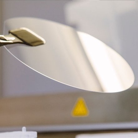
Surface polish Ra < 0.5 nm supports epi-ready growth with minimal defects.
Thermal stability > 1000 °C allows safe high-temperature processing.
Optical transmission from 200 nm–5 µm enables applications from UV to IR.
Low dielectric loss guarantees reliable RFIC and microwave circuit performance.
Mechanical hardness provides durability in aggressive environments.
Technical Specifications of 6-Inch Sapphire Wafer
| Parameter | Specification (Typical) |
|---|---|
| Material Purity | ≥ 99.99% Al₂O₃ single crystal |
| Diameter | 150 mm ± 0.2 mm (≈ 6 inch) |
| Thickness | 1300 µm ± 20 µm (SSP or DSP) |
| Orientation | C-plane (0001) standard; A-, R-, M-plane available |
| Surface Finish | SSP: one epi-ready side Ra < 0.5 nm; DSP: both sides polished |
| TTV / Bow / Warp | ≤ 15–20 µm |
| Primary Flat & Length | A-plane primary flat ≈ 47.5 mm ± 2 mm |
| Edge Profile | SEMI standard bevel or customized |
| Thermal Expansion Coefficient | ∥ C-axis: 6.66 × 10⁻⁶ /°C; ⟂ C-axis: 5.0 × 10⁻⁶ /°C |
| Thermal Conductivity | 30–42 W/(m·K) at ~25 °C |
| Dielectric Constant | ∥ C-axis ≈ 11.5; ⟂ C-axis ≈ 9.3 |
| Dielectric Strength | ~4.8 × 10⁵ V/cm |
| Refractive Index | ~1.77 in visible spectrum |
| Optical Transmission | 200 nm – 5 µm |
| Mohs Hardness | 9 |
Applications of 6-Inch Sapphire Substrate
LED and Optoelectronics
You depend on the 6-inch sapphire wafer for GaN epitaxy in blue, green, and UV LEDs. Because the wafer minimizes lattice mismatch, you obtain higher efficiency and better device yields.
Laser and Photonics
You apply sapphire substrate in UV lasers, detectors, and optical filters. Its transparency across UV–IR makes it ideal for demanding photonic devices.
RF and SOS Devices
You employ sapphire wafer for RFIC and silicon-on-sapphire circuits. Its electrical insulation reduces dielectric loss and enhances high-frequency performance.
MEMS and Sensors
You integrate sapphire substrate into MEMS, pressure sensors, and optical instruments. Its mechanical strength and surface polish ensure accuracy.
Research and Prototyping
You also use 6-inch sapphire wafer in laboratories testing new epitaxy methods or photonic structures, because it provides industrial relevance at a manageable cost.
Processing and Customization
Crystal growers produce sapphire boules through Kyropoulos (KY) or Czochralski (CZ) methods. After slicing, wafers undergo grinding, lapping, and polishing with diamond abrasives. Because of advanced chemical-mechanical polishing (CMP), surfaces reach Ra < 0.5 nm.
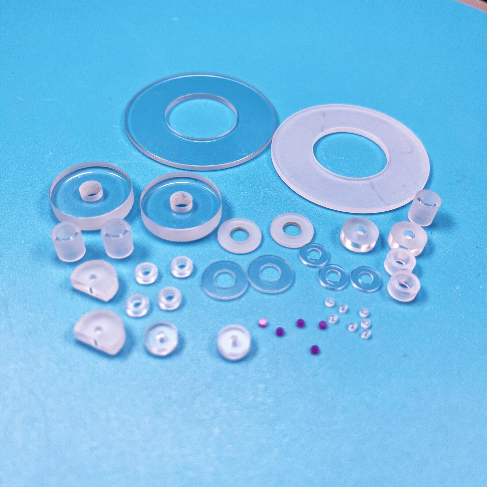
You request customized features such as orientation flats, miscut angles, patterned surfaces, or special thicknesses. You also order SSP or DSP depending on whether one or both sides require epi-ready polish. Thus, you adapt the sapphire wafer precisely to your application.
Why Sapphire Wafer Beats Alternatives
Although SiC and silicon compete in some applications, sapphire remains more cost-effective for optoelectronics. Unlike silicon, sapphire wafer tolerates >1000 °C and provides optical transparency. Unlike SiC, sapphire substrate offers affordability for mass LED production. Unlike glass or quartz, sapphire delivers superior hardness, thermal conductivity, and dielectric strength. Therefore, sapphire wafer holds its position as the most versatile choice for LEDs, lasers, and RF circuits.
Q&A: Focused on Sapphire Wafer
Q: Why is the 6-inch sapphire wafer preferred for LED production?
A: You gain higher throughput and lower cost per device, while maintaining the crystalline quality necessary for GaN epitaxy.
Q: What is the difference between SSP and DSP sapphire wafers?
A: You choose SSP if you need one epi-ready side, and you select DSP when both sides must remain polished for optical or MEMS uses.
Q: Can sapphire wafer endure extreme environments?
A: Yes, you rely on its hardness, chemical inertness, and thermal stability, which make it ideal for aerospace, defense, and high-power electronics.
Q: How does sapphire compare to silicon or SiC?
A: You exploit sapphire’s transparency, durability, and cost-effectiveness, whereas silicon lacks high-temperature resilience and SiC costs more.
Q: Is customization available for 6-inch sapphire substrate?
A: Absolutely, you order custom flats, thickness, bevels, or miscut angles depending on your device requirements.