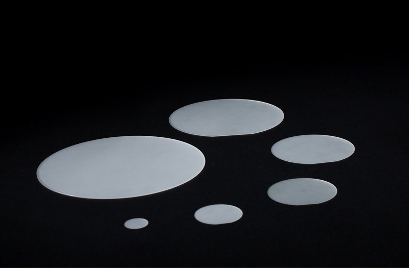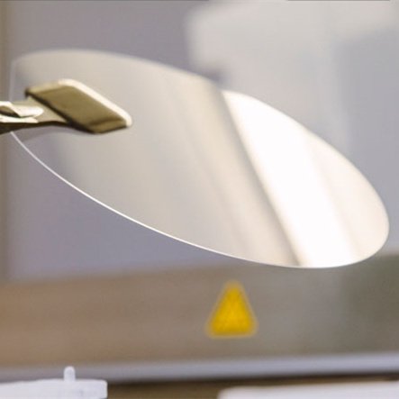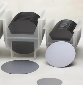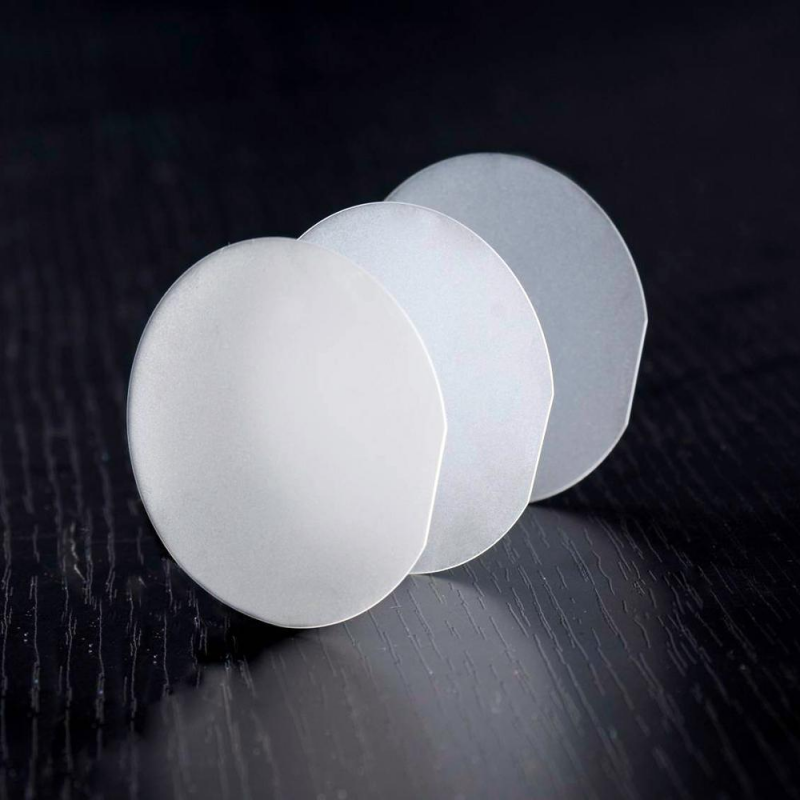

P-grade silicon carbide(SiC)wafer 8inch Product Overview:
Our 8-inch Conductive SiC (Silicon Carbide) Substrate is designed for the most demanding applications in semiconductor fabrication and power electronics, In LED manufacturing, we offer two distinct grades: namely the Zero MPD Production Grade (Z Grade) and the Dummy Grade (D Grade).
Specifically, these grades are designed to meet diverse industry needs while delivering unmatched precision as well as reliability.
SiC substrates are essential for high-performance devices due to their excellent electrical properties and ability to withstand high temperatures and making them ideal for power semiconductors.
Besides these substrates can be used in critical applications like high-power devices and automotive power systems, and RF (Radio Frequency) components.
Key Specifications:
Diameter:
Zero MPD Production Grade (Z Grade): 199.5 mm – 200.0 mm
Dummy Grade (D Grade): 199.5 mm – 200.0 mm
Both grades are designed with highly precise tolerances besides ensuring consistency for high-volume production processes.
Poly-type:
Zero MPD Production Grade (Z Grade): 4H
Dummy Grade (D Grade): 4H
The 4H poly-type is renowned for its robustness and performance in electronic devices.
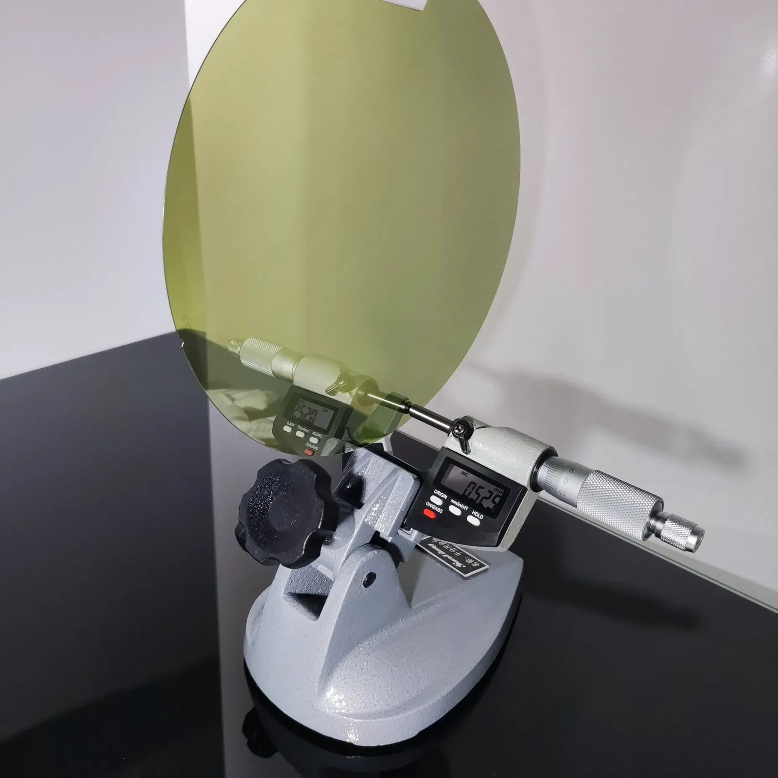
Thickness:
500 µm ± 25 µm
Consistent thickness ensures uniform processing and optimal performance in semiconductor fabrication.
Wafer Orientation:
Zero MPD Production Grade (Z Grade): 4.0° toward <11-20> ± 0.5°
Dummy Grade (D Grade): 4.0° toward <11-20> ± 0.5°
The precise wafer orientation enhances the material’s electrical properties and ensures minimal wafer defects.
Micropipe Density:
Zero MPD Production Grade (Z Grade): ≤ 0.2 cm²
Dummy Grade (D Grade): ≤ 5 cm²
Low micropipe density in the Z Grade ensures higher yield and quality and critical for high-performance devices.
Resistivity:
Zero MPD Production Grade (Z Grade): 0.015 – 0.025 Ω·cm
Dummy Grade (D Grade): 0.015 – 0.028 Ω·cm
The low resistivity values in both grades ensure efficient current flow and especially for high-power applications.
Notch Orientation:
Zero MPD Production Grade (Z Grade): {10-10} ± 5.0°
Dummy Grade (D Grade): {10-10} ± 5.0°
Precision in notch orientation guarantees compatibility with standard processing equipment and systems.
Edge Exclusion:
3 mm for both grades
The edge exclusion standard ensures uniform processing and consistent results throughout wafer production.
LTV / TTV / Bow / Warp:
Zero MPD Production Grade (Z Grade): ≤ 5 µm / ≤ 10 µm / ± 35 µm / 70 µm
Dummy Grade (D Grade): ≤ 10 µm / ≤ 15 µm / ± 50 µm / 100 µm
These tight tolerances on bow and warp, as well as thickness variation, are critical not only for ensuring the wafer’s stability but also for maintaining uniformity in final product applications.
Polish Surface Quality:
Zero MPD Production Grade (Z Grade): Ra ≤ 1 nm andCMP Ra ≤ 0.2 nm
Dummy Grade (D Grade): Ra ≤ 1 nm and CMP Ra ≤ 0.5 nm, which means the surface roughness is extremely low. Furthermore, this promotes excellent adhesion and thus enhances integration with subsequent layers in semiconductor manufacturing processes.
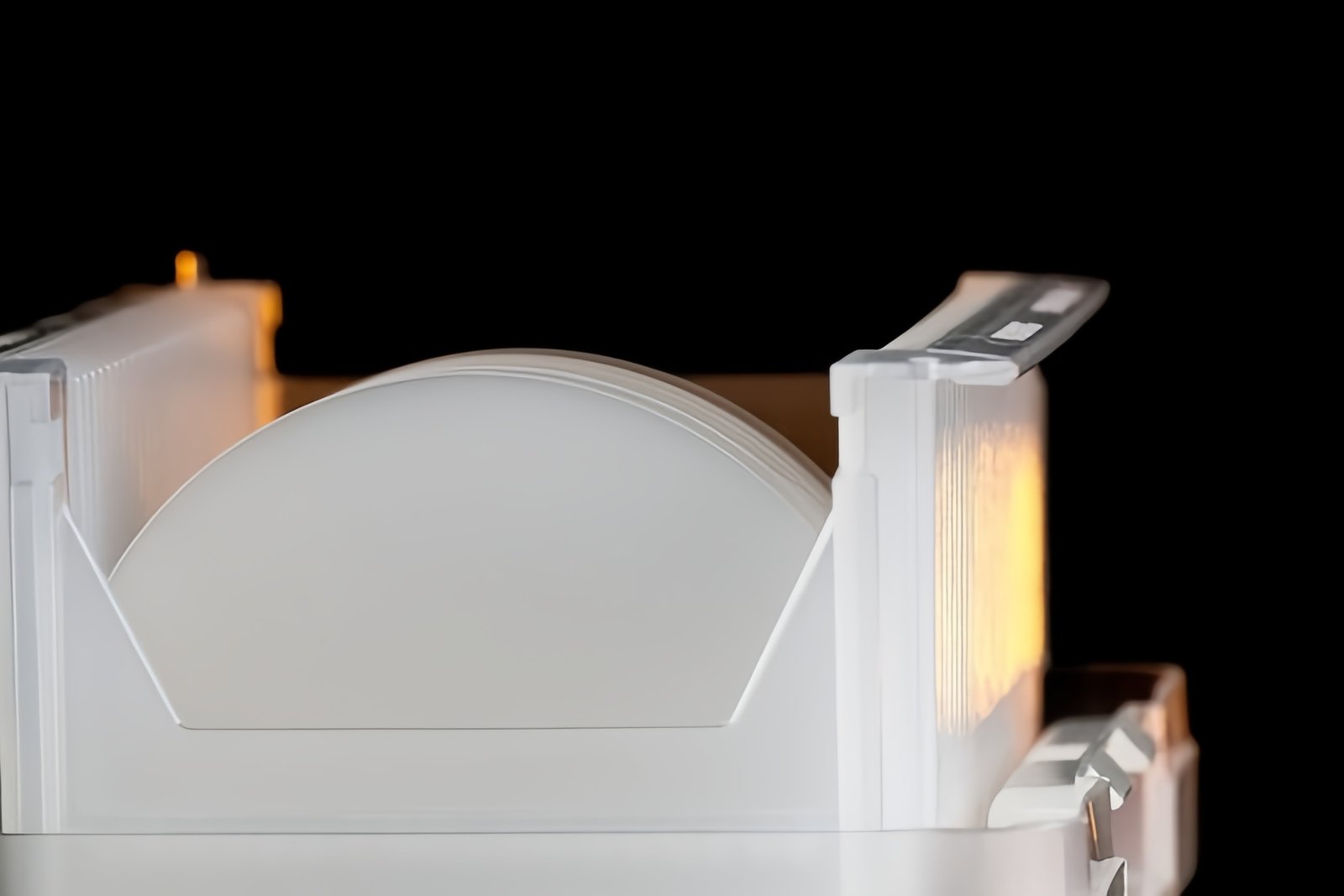
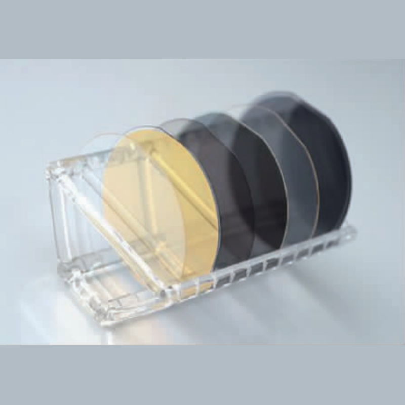
Packaging:
Both grades are available in multi-wafer cassette or single wafer container and allowing flexibility for different production volumes and processing requirements.
| Specification | Zero MPD Production Grade (Z Grade) | Dummy Grade (D Grade) |
|---|---|---|
| Diameter | 199.5 mm – 200.0 mm | 199.5 mm – 200.0 mm |
| Poly-type | 4H | 4H |
| Thickness | 500 µm ± 25 µm | 500 µm ± 25 µm |
| Wafer Orientation | 4.0° toward <11-20> ± 0.5° | 4.0° toward <11-20> ± 0.5° |
| Micropipe Density | ≤ 0.2 cm² | ≤ 5 cm² |
| Resistivity | 0.015 – 0.025 Ω·cm | 0.015 – 0.028 Ω·cm |
| Notch Orientation | {10-10} ± 5.0° | {10-10} ± 5.0° |
| Edge Exclusion | 3 mm | 3 mm |
| LTV / TTV / Bow / Warp | ≤ 5 µm / ≤ 10 µm / ± 35 µm / 70 µm | ≤ 10 µm / ≤ 15 µm / ± 50 µm / 100 µm |
| Roughness | Polish Ra ≤ 1 nm, CMP Ra ≤ 0.2 nm | Polish Ra ≤ 1 nm, CMP Ra ≤ 0.5 nm |
| Edge Cracks by High Intensity Light | Not allowed | Cumulative area ≤ 0.05% |
| Hex Plates by High Intensity Light | Not allowed | Cumulative area ≤ 0.1% |
| Polypype Areas by High Intensity Light | Not allowed | Cumulative area ≤ 3% |
| Silicon Surface Scratches by High Intensity Light | Not allowed | Cumulative length ≤ 30 mm, single length ≤ 2 mm |
| Edge Chips by High Intensity Light | Not allowed | Cumulative area ≤ 3% |
| Threading Screw Dislocation | Not allowed | None permitted, ≥ 0.2 mm width and depth |
| Silicon Surface Contamination by High Intensity Light | Not allowed | Not allowed |
| Packaging | Multi-wafer Cassette or Single Wafer Container | Multi-wafer Cassette or Single Wafer Container |
Why Choose Our SiC Substrate?
High Performance: The Zero MPD Production Grade not only offers low micropipe density but also maintains tight tolerances, thereby ensuring high yield in the production of power devices, high-performance electronics, and even RF components. On the other hand, the Dummy Grade is specifically designed for testing and calibration, as well as other less stringent applications, since it provides a cost-effective solution while still meeting basic operational requirements.
Durability & Longevity: SiC is known for its ability to operate at high temperatures and making these substrates an ideal choice for devices that will be exposed to harsh operating conditions.
Precision Manufacturing: With a focus on minimal surface roughness and optimal resistivity, and precise wafer orientation and for the 8-inch SiC substrate ensures the highest levels of quality and reliability besides efficiency.
Flexibility for Various Applications: Whether you require high-quality production wafers (Z Grade) or cost-effective dummy wafers (D Grade) for testing purposes
besides this substrate product can serve a wide range of applications and from power semiconductors to automotive electronics.
Customization Available: We understand that different industries have unique requirements besides we are ready to customize these substrates based on your specific needs.
Applications:
Power Electronics: Power modules and power diodes, and MOSFETs in high-power applications.
Semiconductor Devices: Devices used in telecommunications and automotive, and industrial equipment.
LED and RF Devices: Ensuring superior performance and reliability in high-power LED and RF device applications.