


300mm Sapphire Wafer: A Comprehensive Guide for High-Performance Applications
Introduction
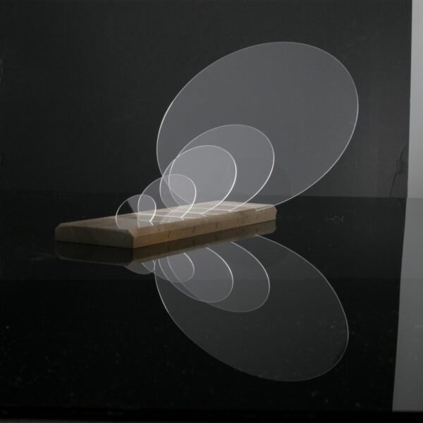
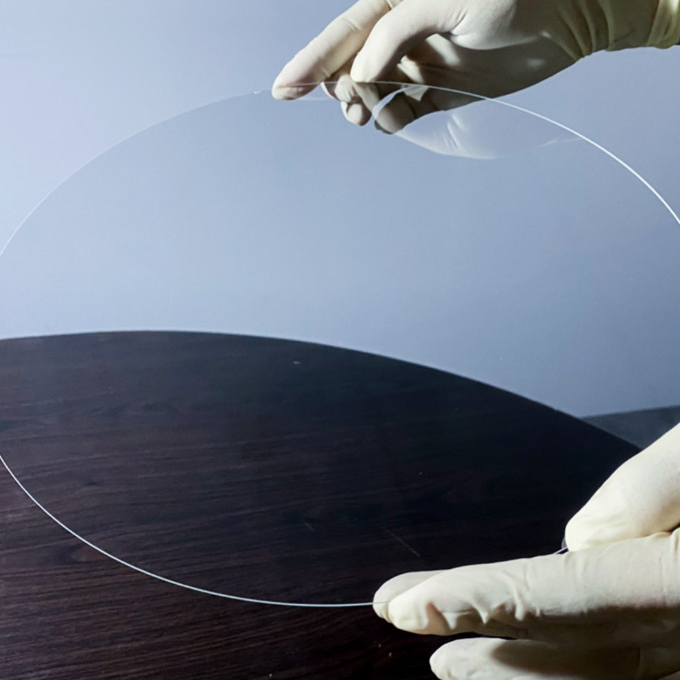
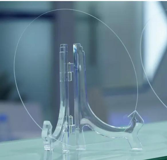
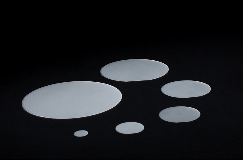
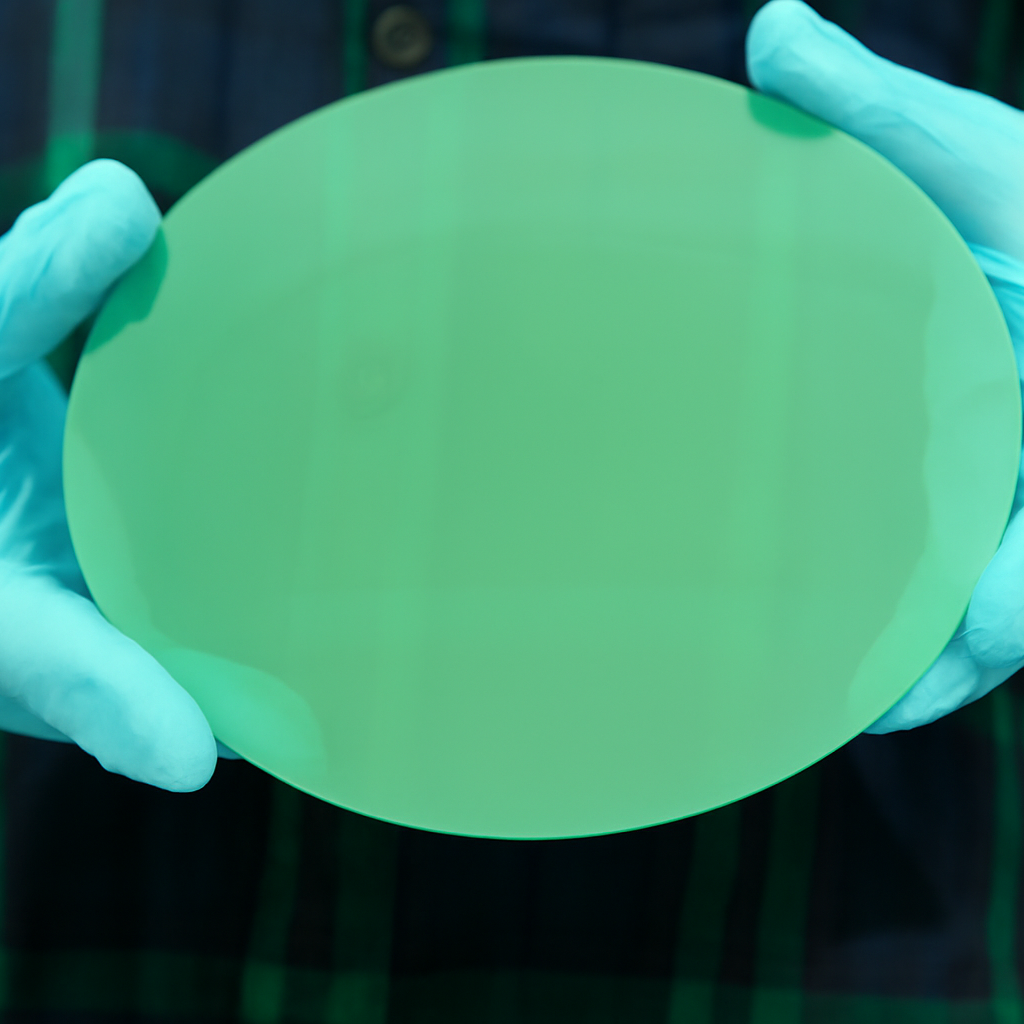
The 300mm sapphire wafer plays a crucial role in industries such as semiconductors, LED manufacturing, and optical devices. With its high purity, exceptional thermal conductivity, and long-lasting durability, this material has become the substrate of choice for advanced technologies. In this article, we will examine the 300mm sapphire wafer, its specifications, its manufacturing process, and common industry questions. We will also highlight the key factors to consider when selecting this material for your projects.
Key Specifications of the 300mm Sapphire Wafer
To choose the right 300mm sapphire wafer for your application, understanding its specifications is crucial. Below, we provide a breakdown of the most important parameters:
| Parameter | Production-1 | Production-2 | Production-3 |
|---|---|---|---|
| Material | >99.99%, High Purity, Mono-crystalline AI2O3 (KY) | High Purity, Mono-crystalline AI2O3 (KY) | >99.999%, High Purity, Mono-crystalline AI2O3 (KY) |
| Diameter | 300mm±0.2mm | 300mm±0.2mm | 300mm±0.2mm |
| Thickness | 1000mm±50mm | 800mm±50mm | 1200mm±50mm |
| Orientation | C-Plane(0001) off-set | C-Plane(0001) off-set | C-Plane(0001) off-set |
| Off-set Angle toward M– | 0.0 ±0.3 degree | 0.0 ±0.3 degree | 0.0 ±0.3 degree |
| Notch Orientation | A-Plane(0001) 0°±1° | A-Plane(0001) 0°±1° | A-Plane(0001) 0°±1° |
| Notch Depth | 1.0–1.25mm | 1.0–1.25mm | 1.0–1.25mm |
| Bevel | T-type 200um±100um | T-type 200um±100um | T-type 200um±100um |
| TTV | ≤25μm | ≤25μm | ≤25μm |
| BOW | ≤35μm | ≤35μm | ≤35μm |
| WARP | ≤120μm | ≤120μm | ≤120μm |
| Scratch | 5 scratches within 2mm of the edge, 3 beyond 2mm, slight scratches ≤3mm | 5 scratches within 2mm of the edge, 3 beyond 2mm, slight scratches ≤3mm | 5 scratches within 2mm of the edge, 3 beyond 2mm, slight scratches ≤3mm |
| Bubbles/Pits | ≤4 bubbles with diameter of 10-60µm | ≤4 bubbles with diameter of 10-60µm | ≤4 bubbles with diameter of 10-60µm |
| Chips | ≤0.2mm | ≤0.2mm | ≤0.2mm |
| Laser Mark | None | None | None |
| Packing | CRC100 packed, 1pc/box | CRC100 packed, 1pc/box | CRC100 packed, 1pc/box |
The Manufacturing Process of 300mm Sapphire Wafer
Producing the 300mm sapphire wafer involves several carefully controlled steps. These steps ensure that the wafer meets the high standards required for various high-performance applications. Let’s break down the process:
Material Selection
The process begins with selecting high-purity sapphire. Manufacturers typically choose materials with a purity of more than 99.99%, ensuring optimal performance in sensitive applications.
Crystal Growth
The Czochralski process plays a crucial role in crystal growth by enabling precise control over the size and orientation of the crystal. This method ensures that the wafers maintain uniformity, which is essential for meeting the stringent requirements of industries like LEDs, semiconductors, and optical devices. As a result, manufacturers can produce high-quality sapphire wafers that meet the performance standards required for advanced applications.
Polishing Process
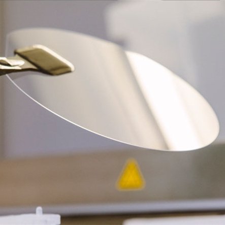
After the crystal growth, the wafers undergo double-side polishing to achieve a smooth and uniform surface. This process is critical for ensuring that the wafers meet the high-precision needs of industries such as semiconductors and optoelectronics. In addition, the polishing enhances the wafers’ surface quality, ensuring they are ready for use in applications that demand strict dimensional accuracy and flawless surfaces.
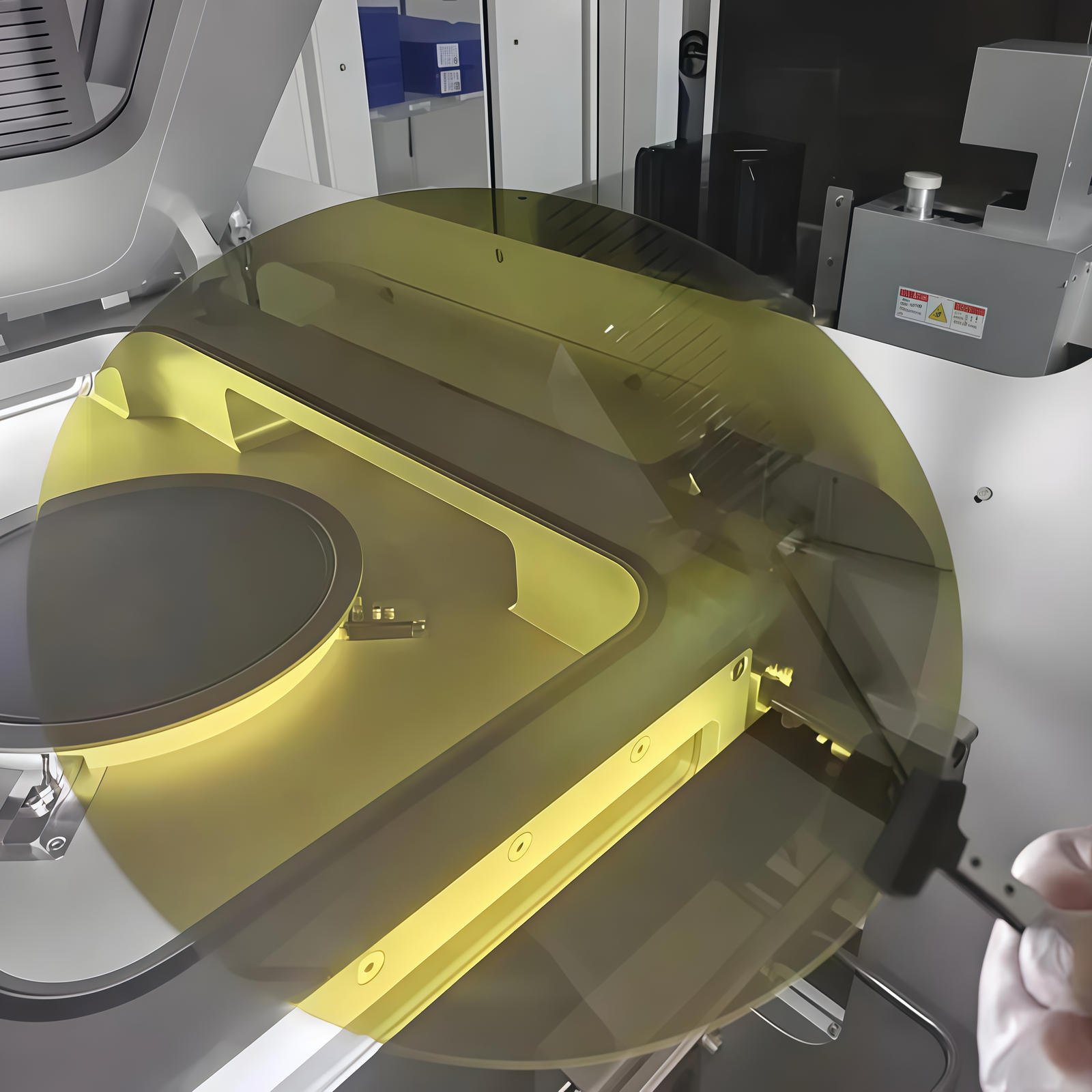
Testing and Inspection
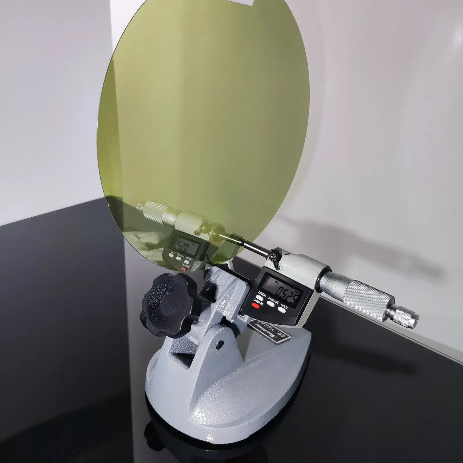
Following the polishing process, the wafers undergo thorough testing and inspection. Manufacturers carefully examine them for defects, such as scratches, chips, and bubbles, which could impact their performance. Moreover, they measure TTV (Total Thickness Variation) and BOW to assess the uniformity and flatness of the wafers. This step ensures that the wafers are suitable for high-precision applications and meet the necessary quality standards.
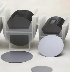
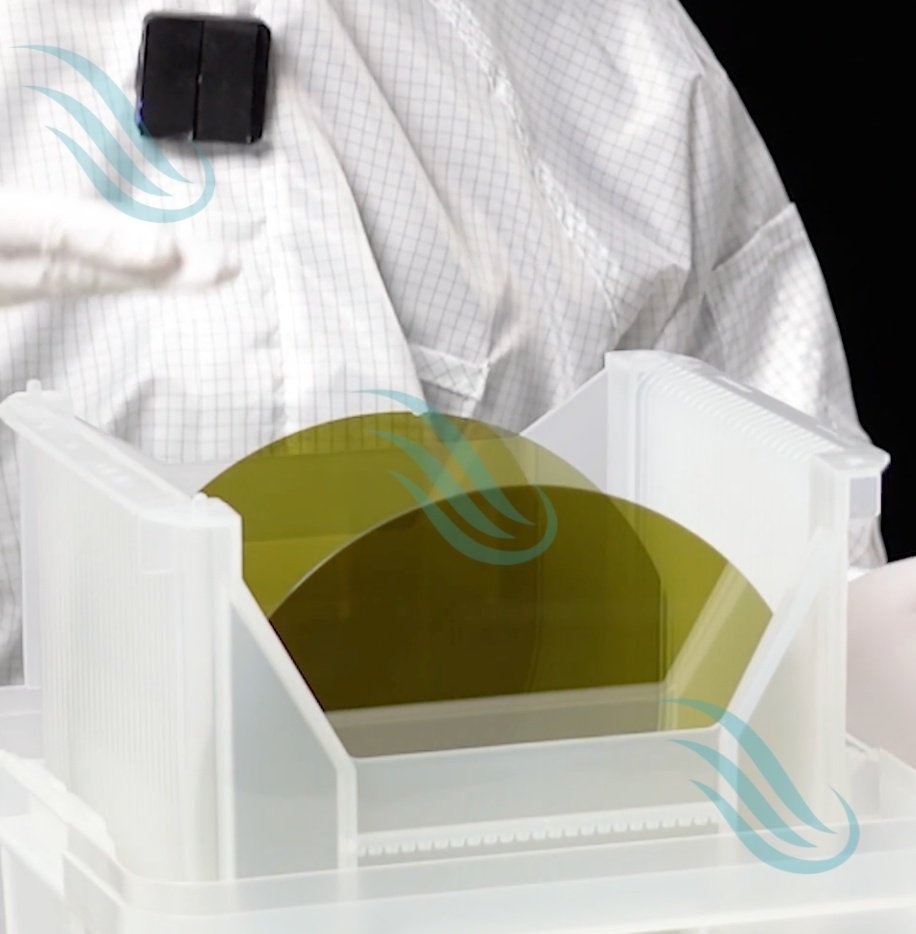
Packaging
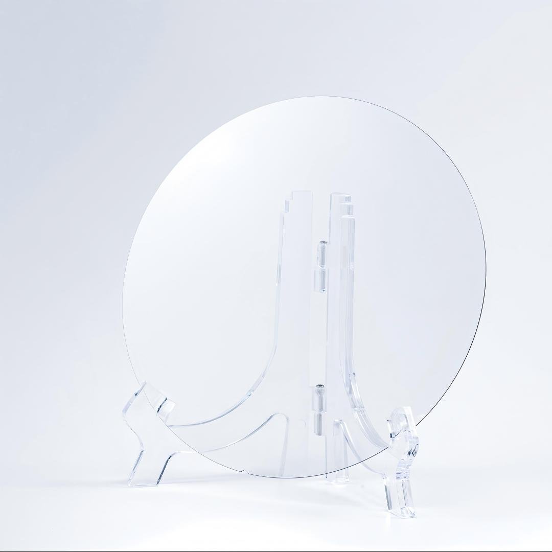
Finally, the wafers are carefully packaged to prevent contamination and physical damage during transportation. This step is essential as it protects the wafers from external factors that could compromise their integrity. Therefore, proper packaging guarantees that the wafers remain intact and are ready for use in advanced technologies upon delivery.
Q&A 300mm Sapphire Wafer
Q1: Why is the 300mm sapphire wafer important for LED and semiconductor applications?
A: The 300mm sapphire wafer is crucial for these applications due to its excellent thermal conductivity, which helps dissipate heat efficiently. This is especially important in high-power LEDs and semiconductors where heat management is essential for long-term performance and reliability. Additionally, its optical transparency enhances the light emission in LEDs, making it an ideal substrate for such applications.
Q2: How does the larger size of the 300mm sapphire wafer benefit production?
A: The larger size allows for higher production yields, as manufacturers can produce more devices from a single wafer. Larger wafers also offer a more uniform surface, which is critical for maintaining precision in applications such as semiconductors and LED manufacturing.
Q3: What role does the thickness of the sapphire wafer play in its performance?
A: The thickness directly affects both the mechanical strength and thermal stability of the wafer. Thicker wafers can handle more stress and heat, making them ideal for high-power applications. In contrast, thinner wafers are better suited for optical devices and precision electronics, where the primary focus is on light transmission rather than strength or heat resistance.
Q4: Can the 300mm sapphire wafer be used in high-power LED manufacturing?
A: Yes, manufacturers commonly use the 300mm sapphire wafer in high-power LED applications. Due to its superior thermal conductivity, the wafer efficiently dissipates heat, which helps maintain the LED’s performance over time. Additionally, its optical clarity makes it an excellent choice for high-performance lighting, further enhancing the overall quality of the LED output.
Q5: How does the 300mm sapphire wafer compare to silicon wafers?
A: While silicon wafers are cheaper and more commonly used in general electronics, sapphire wafers offer superior thermal management and optical properties. These advantages make sapphire wafers ideal for LED and optical device applications, where thermal stability and light transmission are crucial.
Q6: What should manufacturers consider when selecting a 300mm sapphire wafer?
A: Key factors to consider include wafer thickness, surface quality, TTV, and BOW. Defects such as scratches, bubbles, and chips should also be examined, as they can affect the wafer’s performance in high-precision applications.
Q7: Can the 300mm sapphire wafer be customized for specific applications?
A: Yes, manufacturers offer customization options. Customers can adjust parameters like thickness, orientation, surface finish, and defect tolerance to suit their needs for specific LEDs, semiconductors, or optical components.
Conclusion
The 300mm sapphire wafer is a vital material in the production of LEDs, semiconductors, and optical devices. Its thermal conductivity, mechanical strength, and optical transparency make it an ideal substrate for high-performance applications. By understanding the specifications, manufacturing process, and answering common questions, you can make an informed decision when selecting the 300mm sapphire wafer for your next project.
