
8-inch SiC Wafer: Revolutionizing Power Electronics
Introduction to 8-inch SiC Wafers
More and more industries are recognizing the exceptional performance of 8-inch SiC wafers in various power applications, such as electric vehicles, renewable energy systems, and aerospace technologies. As a result, these wafers are becoming essential for high-performance devices in these sectors.
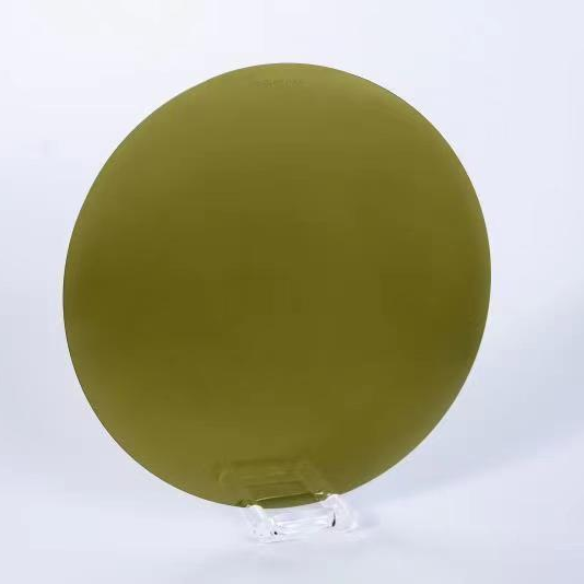
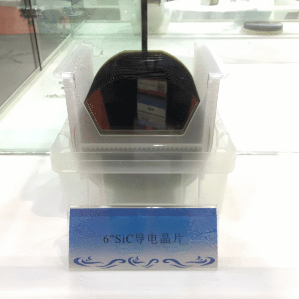
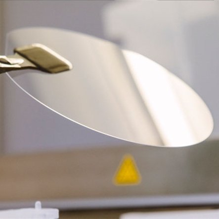
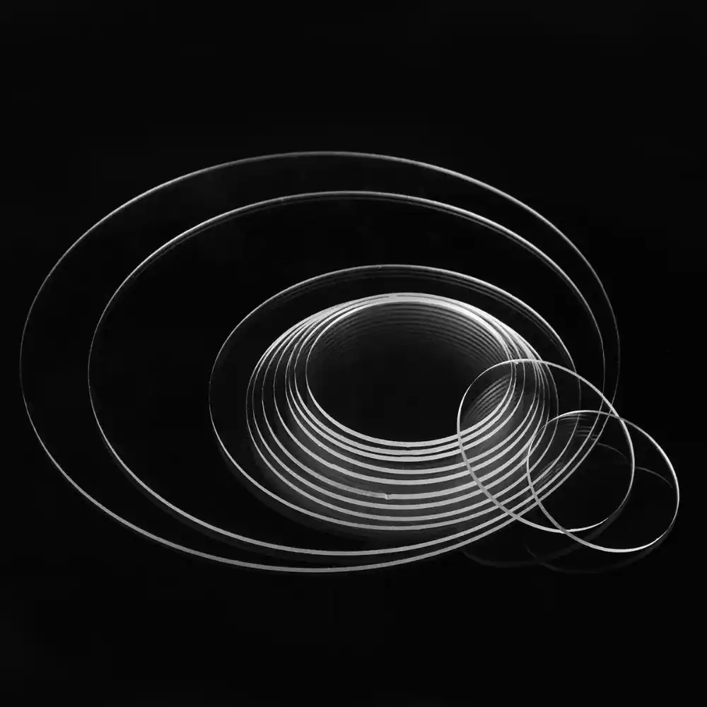
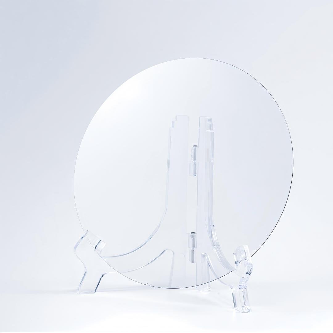
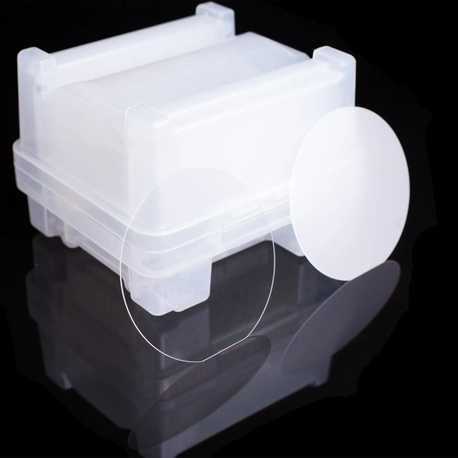
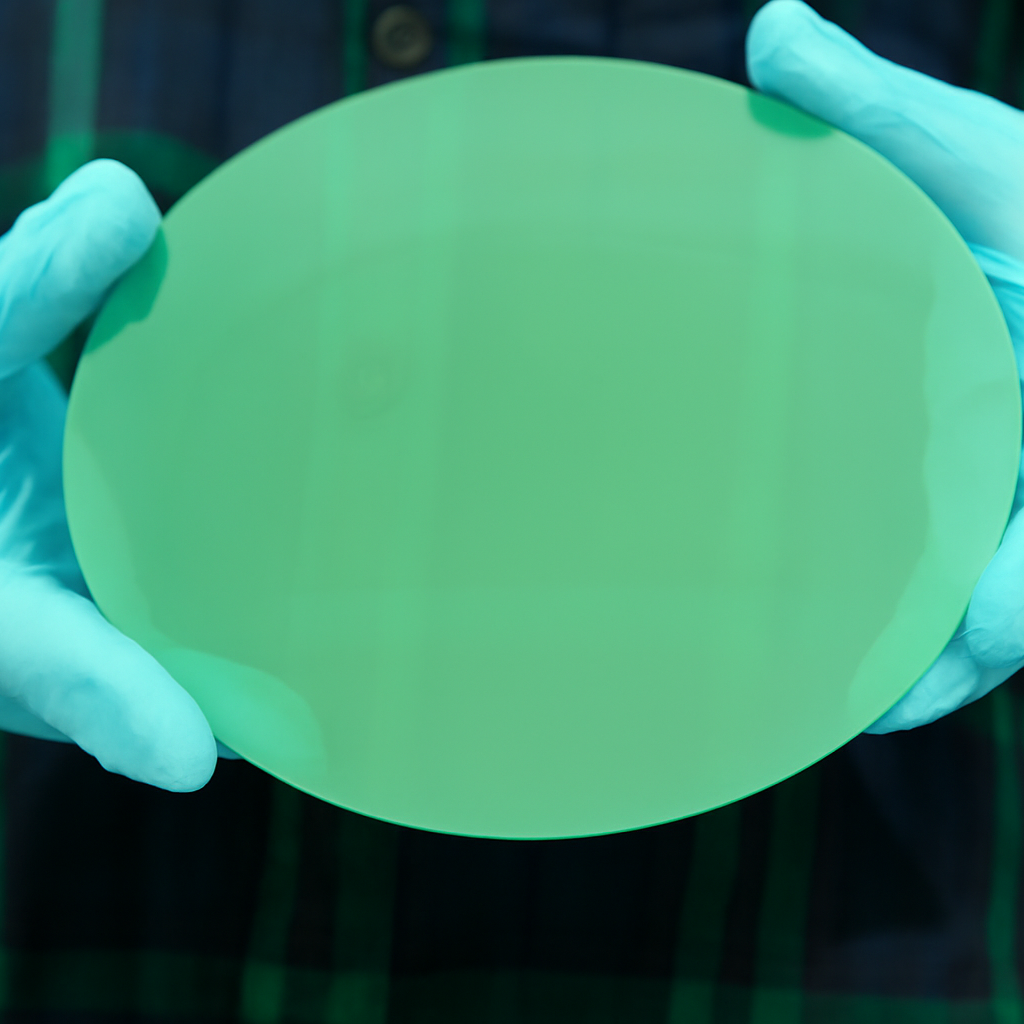
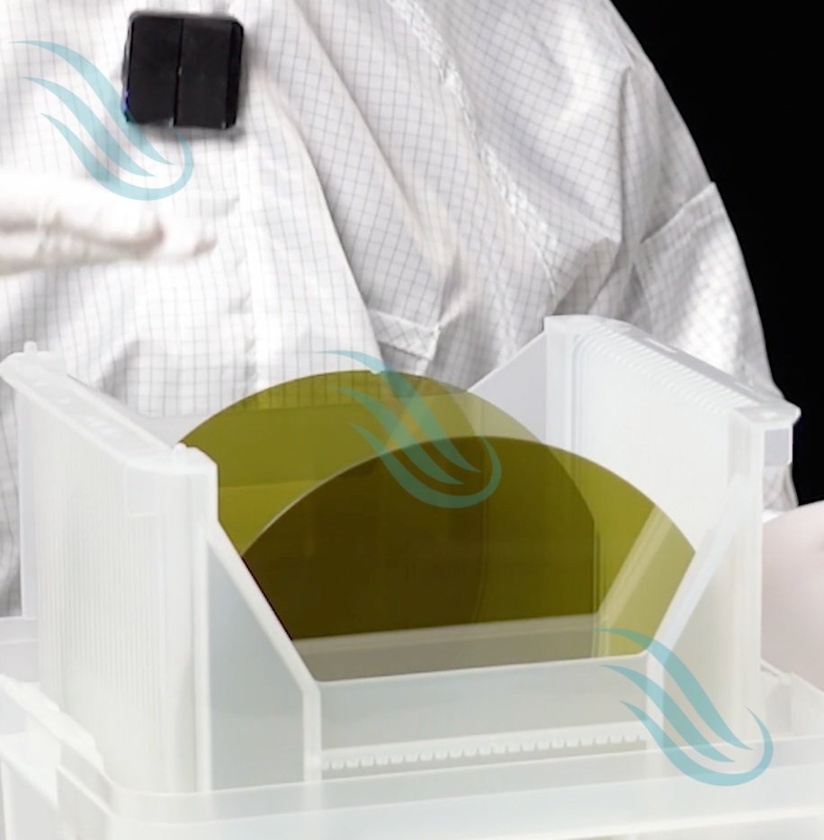
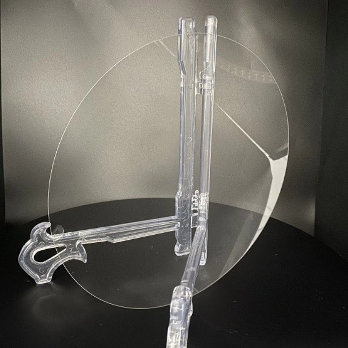
8-inch SiC wafers are used in power devices like diodes, MOSFETs, and other semiconductor components. These wafers offer improved efficiency, higher thermal conductivity, and superior voltage handling capabilities compared to traditional silicon wafers. At Guangdong Vastron Technology Co., Ltd., we produce 8-inch SiC wafers that meet industry standards, ensuring that your power devices can perform at their best.
| Specification | Details |
|---|---|
| Diameter | 199.5 mm – 200.0 mm |
| Crystal Structure | 4H |
| Thickness | 500 µm ±25 µm |
| Doping Type | P-type |
| Orientation | ±11°-20′ (±40°±0.5°) |
| Resistivity | ≤ 0.2 Ω·cm² |
| Electrical Resistance | 0.015 – 0.025 Ω·cm |
| Notch Position | (10-10) ±15° |
| Warp | ≤ 3 µm |
| Bow | ≤ 3 µm |
| Surface Finish | CMP Ra ≤ 0.2 µm |
| Wafer Flatness | ≤ 0.05% |
| Dislocation Density (TSD) | ≤ 300 cm⁻² |
| Package | Customized packaging as per requirement |
Why Choose 8-inch SiC Wafers?
The use of 8-inch SiC wafers is a game-changer for power electronics. With an increased wafer diameter, these wafers allow for a higher yield of chips, reducing costs per chip. Moreover, their enhanced properties make them ideal for high-frequency, high-voltage, and high-temperature environments. Unlike standard silicon wafers, 8-inch SiC wafers offer superior performance in power conversion, energy efficiency, and device longevity.
Here are some key reasons why 8-inch SiC wafers are highly valued in the industry:
Efficiency: 8-inch SiC wafers have a significantly higher power density and efficiency than their silicon counterparts.
Durability: They can withstand higher temperatures and voltages, making them suitable for demanding applications.
Cost-effective: Due to their larger size, 8-inch SiC wafers help reduce manufacturing costs by improving yield per wafer.
Manufacturing Process of 8-inch SiC Wafers
To produce 8-inch SiC wafers, the process starts with a 6-inch 4H-SiC seed crystal. Through the physical vapor transport (PVT) method, the SiC crystal is expanded to a diameter of 209 mm. After growing the crystal, we carefully cut, grind, polish, and clean it to achieve the final 8-inch SiC wafer size.
During this process, several important factors come into play to ensure optimal wafer quality:
Crystal growth: We carefully control the temperature, pressure, and atmosphere to ensure uniform crystal growth.
Wafer Cutting and Polishing: We cut the wafer using a multi-wire saw to achieve the initial dimensions. Next, we perform grinding and polishing to refine the surface, ensuring it reaches the required flatness and surface quality. This step is essential to prepare the wafer for precise applications, and we carefully monitor each stage to ensure the highest level of accuracy.
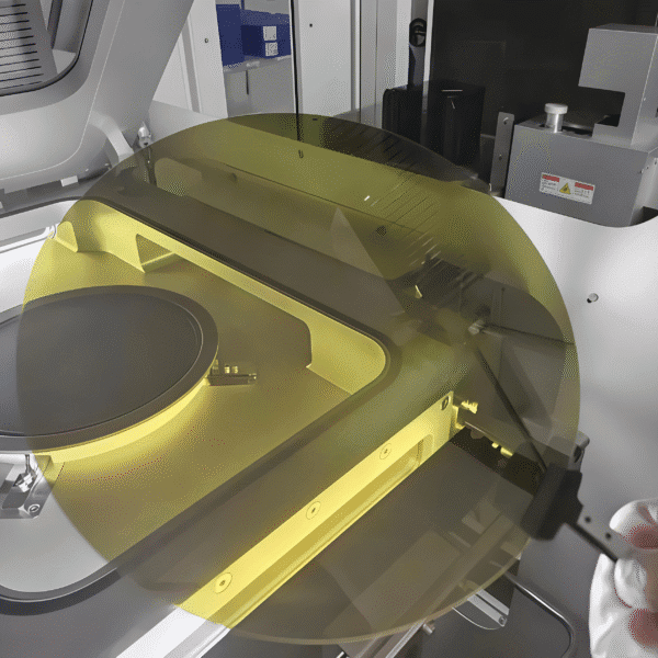
Quality Control: After completing the production process, we rigorously test each 8-inch SiC wafer for its electrical properties, crystal structure, and surface quality. We use advanced testing equipment to evaluate key aspects such as resistivity, crystal orientation, and surface finish, ensuring that every wafer meets our strict performance standards before it reaches our customers.
Key Benefits of 8-inch SiC Wafers
High Efficiency: These wafers offer significant energy efficiency improvements in power conversion, which reduces energy loss in various devices.
Superior Thermal Conductivity: SiC materials can withstand higher temperatures, improving the overall thermal management of devices.
Enhanced Voltage Handling: SiC wafers are designed to handle high voltages, which is crucial for power devices in industries like automotive and renewable energy.
Detailed Characterization of 8-inch SiC Wafers
At Guangdong Vastron Technology Co., Ltd., we take quality seriously. We use several testing methods to ensure our 8-inch SiC wafers meet the highest standards:
Raman Spectroscopy: This method checks the crystal structure and purity. We ensure that our wafers have a 100% 4H-SiC crystal structure, which guarantees optimal performance.
X-ray Diffraction: This testing measures the wafer’s crystal quality, confirming that it meets industry standards for flatness and smoothness.
Micro-pipe Density: A lower micro-pipe density (0.04 cm⁻²) ensures that the wafer is free from defects, which would negatively affect device performance.
Electrical Resistivity: We measure the resistivity of the wafers to ensure proper conductivity for power devices.
Stress Testing: Using polarization stress analyzers, we test the stress distribution across the wafer, confirming that our 8-inch SiC wafers have minimal stress, ensuring device longevity.
Dislocation Density: By analyzing dislocations, we verify that the wafers are free from structural defects.
Applications of 8-inch SiC Wafers
8-inch SiC wafers are used across a wide range of applications due to their excellent performance in extreme conditions. Some key applications include:
Electric Vehicles (EVs): Power electronics in EVs rely on SiC devices for efficient power conversion and energy savings.
Solar Power: Inverters used in solar energy systems benefit from the high efficiency of 8-inch SiC wafers.
Aerospace: SiC components in satellite systems ensure reliable performance in extreme environments.
Industrial Equipment: From power converters to motor control, SiC wafers help industrial applications achieve higher energy efficiency.
Why Guangdong Vastron Technology Co., Ltd. for 8-inch SiC Wafers?
At Guangdong Vastron Technology Co., Ltd., we combine years of expertise with cutting-edge technology to provide high-quality 8-inch SiC wafers. Our wafers undergo rigorous testing to ensure they meet the highest standards for power devices in various industries.
Key Advantages:
Advanced Technology: We use the latest methods and equipment in the production of our 8-inch SiC wafers.
Customization: We can provide wafers with tailored specifications to meet your unique requirements.
Global Supply: We supply high-quality wafers to clients around the world, ensuring the best performance for their power devices.
Conclusion
In conclusion, 8-inch SiC wafers play a vital role in advancing power electronics by offering significant improvements in efficiency, durability, and cost-effectiveness. These wafers excel in high-performance applications, enabling the development of more reliable and energy-efficient devices. With Guangdong Vastron Technology Co., Ltd., you can confidently rely on our advanced manufacturing processes and strict quality control to ensure that our wafers consistently meet the highest industry standards. As a result, our wafers provide exceptional performance for your power devices, making them the ideal choice for industries like electric vehicles, renewable energy, and more.
Core Q&A for 8-inch SiC Wafers
Q1: What are 8-inch SiC wafers used for?
A1: 8-inch SiC wafers are primarily used in power electronic devices such as diodes, MOSFETs, and IGBTs, which are essential components in industries like electric vehicles, renewable energy, and aerospace. These wafers enable efficient power conversion and are key to the development of high-performance devices in these rapidly growing sectors.
Q2: Why are 8-inch SiC wafers better than silicon wafers?
A2: SiC wafers outperform traditional silicon wafers in various critical areas. They offer superior performance in high-temperature, high-voltage, and high-frequency environments, which silicon wafers cannot handle as effectively. SiC wafers have higher thermal conductivity, which improves heat dissipation, and higher breakdown voltage, which allows them to withstand greater electrical stress. Moreover, they feature lower energy loss, making them more efficient, especially in power devices.
Q3: How are 8-inch SiC wafers manufactured?
A3: We produce 8-inch SiC wafers using the physical vapor transport (PVT) method. We begin by expanding a 6-inch seed crystal to 8 inches. During production, we cut, grind, polish, and clean the crystal to meet the desired specifications. The wafer undergoes several stages of precision processing to ensure it has the right dimensions, flatness, and surface quality, meeting high industry standards.
Q4: What makes Guangdong Vastron Technology Co., Ltd. stand out in SiC wafer production?
A4: Guangdong Vastron Technology Co., Ltd. stands out due to its advanced production technologies, rigorous quality control, and years of expertise in SiC wafer manufacturing. We leverage cutting-edge techniques and ensure that all our 8-inch SiC wafers meet the highest industry standards. Furthermore, we offer customizable solutions to cater to specific client needs, ensuring that our products not only meet but exceed customer expectations in a wide range of applications.
Q5: What are the benefits of using 8-inch SiC wafers in electric vehicles?
A5: 8-inch SiC wafers significantly enhance energy conversion efficiency and power density in electric vehicle inverters and chargers. This improvement results in lower energy loss, which is essential for extending the battery life of electric vehicles. Additionally, SiC wafers help improve overall system performance, providing higher efficiency and reliability in power electronics. As a result, electric vehicles benefit from faster charging times, longer operational lifespans, and reduced energy consumption.

