
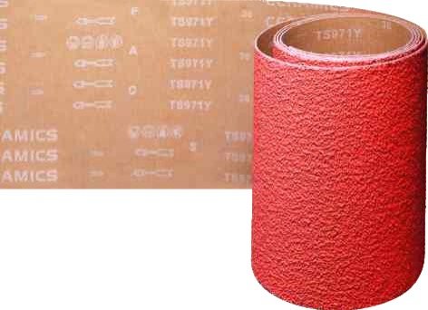
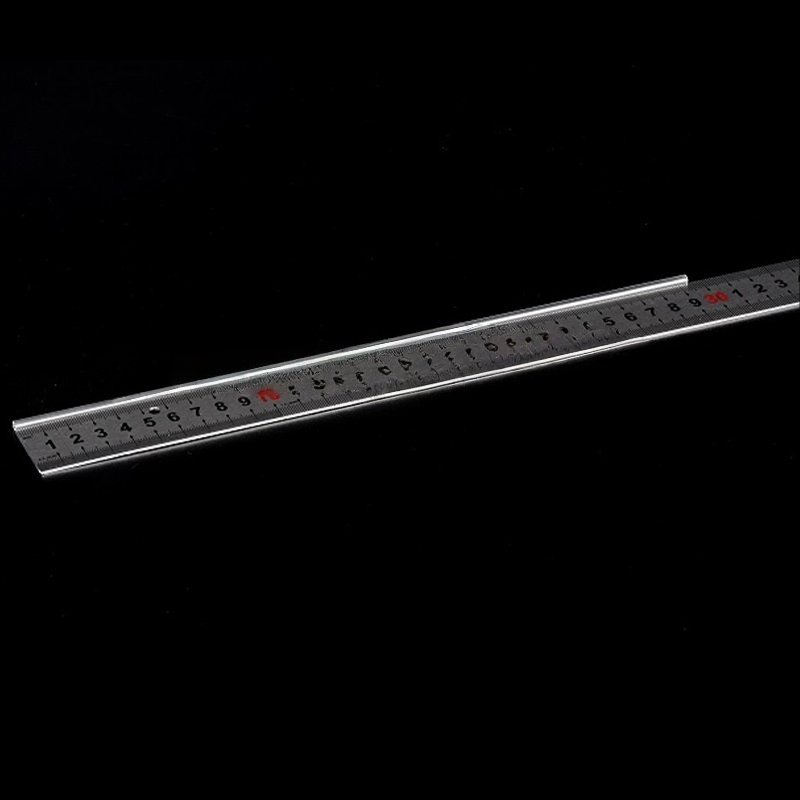
4H Semi-Insulating SiC Wafer – High Resistivity for RF & Power Applications
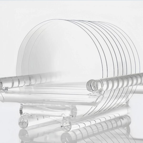
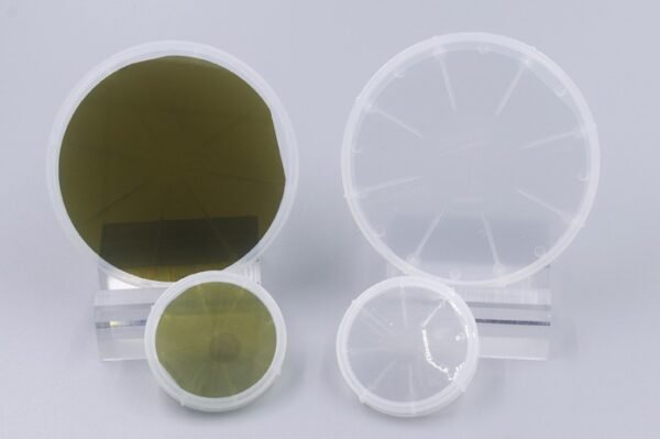
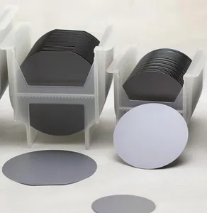
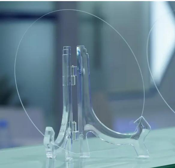
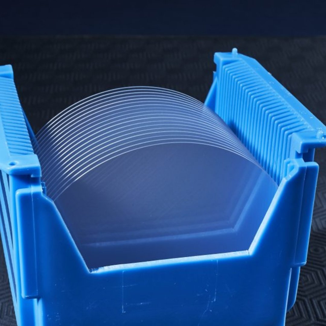
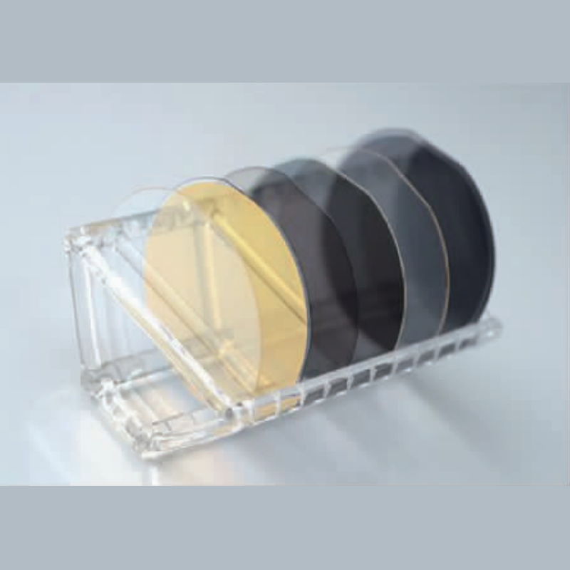
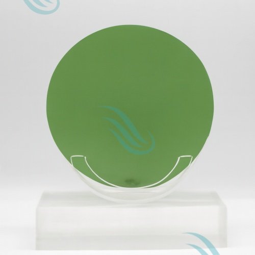
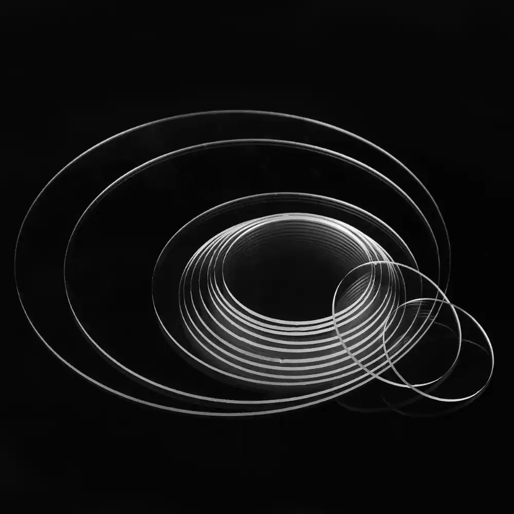
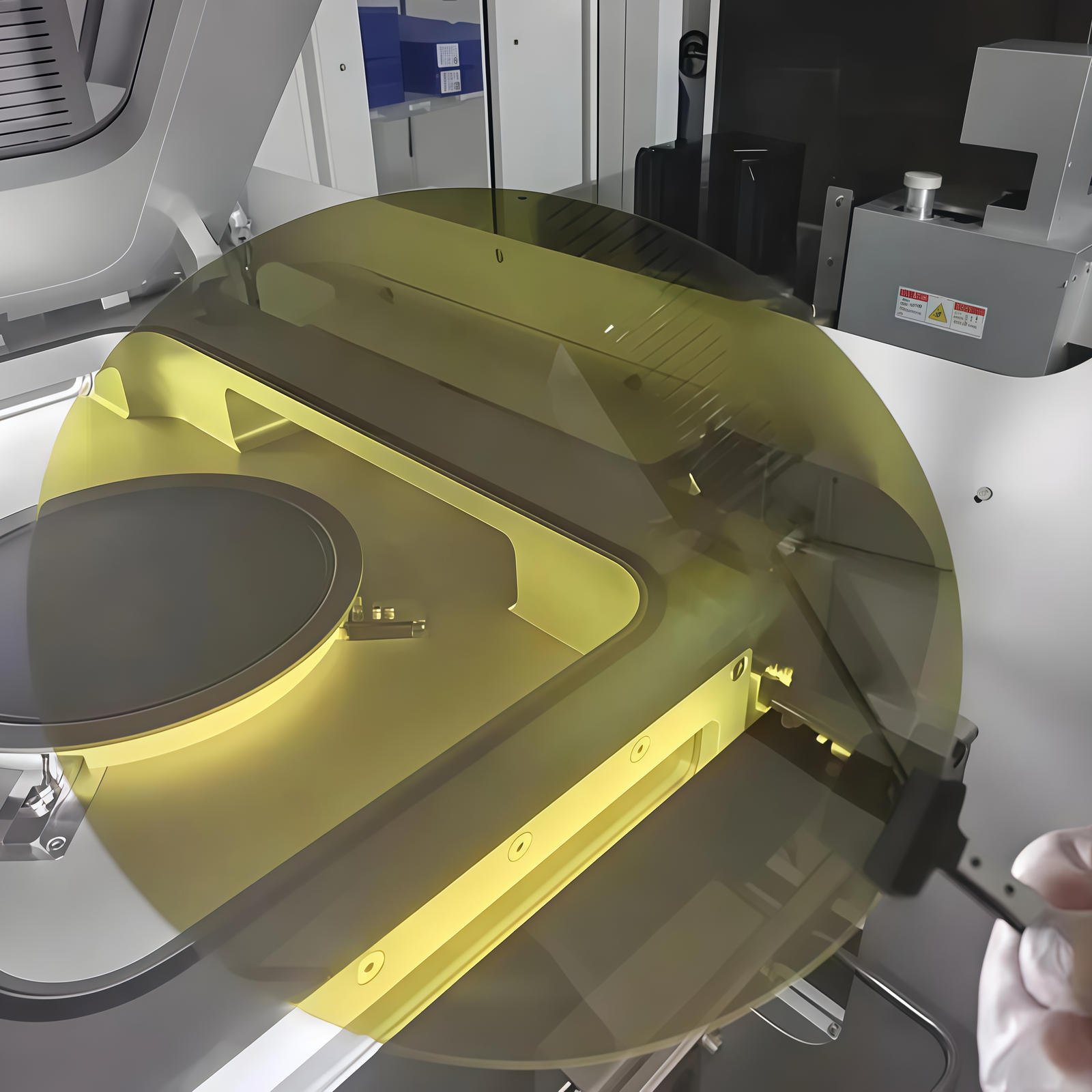
The 4H Semi-Insulating Silicon Carbide (SiC) wafer is a leading substrate for next-generation RF, microwave, and high-power electronics. Because of its ultra-high resistivity (>1×10⁵ Ω·cm), excellent crystalline quality, and availability in 2-inch, 3-inch, 4-inch, 6-inch, and 8-inch diameters, it is now widely adopted by both research institutions and large-scale semiconductor manufacturers.
Moreover, with the rapid expansion of 5G base stations, aerospace radar, satellite communication, and electric vehicles (EVs), the demand for large-diameter semi-insulating SiC wafers continues to rise. Consequently, 8-inch wafers have become the new focus of the global semiconductor industry.
Key Features of 4H Semi-Insulating SiC Wafer
| Parameter | Specification Example | Benefit for Users |
|---|---|---|
| Crystal Polytype | 4H | Stable performance for RF & power devices |
| Resistivity | >1×10⁵ Ω·cm | Minimizes RF loss, ideal for microwave use |
| Diameter | 2″, 3″, 4″, 6″, 8″ | Flexible for research and mass production |
| Surface | Epi-ready, polished | Suitable for epitaxy and device fabrication |
| Grade | Research Grade / Prime Grade | Meets both R&D and industrial needs |
In addition, the wafers are produced under strict quality control, ensuring low defect density and high uniformity. As a result, customers achieve higher device yield and superior reliability.
Why Choose Semi-Insulating 4H-SiC Wafers?
First, semi-insulating wafers provide very high resistivity, which reduces parasitic conduction and improves RF device performance. Consequently, they are essential for GaN-on-SiC HEMTs used in 5G and defense radar.
Second, since 4H-SiC combines a wide bandgap with high thermal conductivity, it supports high-power operation while maintaining efficient heat dissipation. Furthermore, the transition from 6-inch to 8-inch wafers allows higher throughput and lower cost per device.
Finally, compared with sapphire or GaAs substrates, 4H semi-insulating SiC offers greater thermal stability and mechanical strength, which leads to longer device lifetimes.
Applications of 4H Semi-Insulating SiC Wafers
Because 4H semi-insulating SiC combines ultra-high resistivity, wide bandgap, and excellent thermal conductivity, it enables a broad set of RF, microwave, and photonics applications. Moreover, manufacturers can scale from 2″/3″ R&D lines to 4″/6″ pilot runs and, increasingly, to 8″ for cost-efficient mass production. Consequently, device makers gain both performance and yield advantages.
1) RF Front-Ends for 5G/6G (GaN-on-SiC HEMTs)
Engineers widely select semi-insulating 4H-SiC for GaN-on-SiC power amplifiers, LNAs, and RF switches used in macro base stations, small cells, and massive-MIMO arrays. Because the substrate’s high resistivity suppresses parasitic conduction, designers achieve lower RF loss, higher PAE, and better linearity across sub-6 GHz to mmWave bands. Furthermore, the superior thermal conductivity of SiC improves heat spreading under high output power, which, in turn, extends device lifetime.
Typical stack: Epi-ready 4H-SI SiC → GaN/AlGaN HEMT epitaxy → PA/LNA fabrication
Recommended diameters: 4″/6″ for mainstream; 8″ for advanced capacity and cost per die
Suggested spec: Resistivity >1×10⁵ Ω·cm; Si-face CMP; off-cut for GaN epitaxy
2) Aerospace & Defense Radar (AESA T/R Modules)
Modern X-band, S-band, and L-band AESA systems demand high power density and reliability. Therefore, GaN-on-SiC on semi-insulating substrates remains the go-to choice for T/R modules, jammers, and EW payloads. Additionally, 4H-SiC tolerates harsh thermal cycles and elevated junction temperatures, which supports rugged, long-mission profiles.
Benefits: Higher power at bandwidth, improved mean-time-to-failure, stable thermal performance
Diameters: 4″/6″ for qualified lines; 8″ for next-gen radar programs
3) Satellite & Space Communications (Ku/Ka-Band)
Because space payloads operate at Ku/Ka-band with strict SWaP-C limits, designers prioritize high efficiency and thermal robustness. Consequently, 4H-SI SiC substrates for GaN PAs and LNAs deliver low loss, excellent heat removal, and strong reliability under radiation stress. Moreover, 8″ accelerates wafer-level throughput for constellations.
Use cases: Transponders, high-throughput payloads, inter-satellite links
Focus: Low RF loss, tight wafer uniformity, epi-ready finish
4) RF Filters & Resonators (AlN/ScAlN-on-SiC BAW/FBAR)
For high-power, thermally demanding RF front-ends, AlN/ScAlN thin-films on SI-SiC enable high-Q resonators and low insertion-loss BAW filters. Because SiC removes heat efficiently, filters maintain performance at elevated power. Furthermore, designers reduce drift and maintain tighter frequency control across temperature.
Advantages: Better Q×f, lower self-heating, improved reliability versus sapphire or Si
Diameters: 4″/6″ today; 8″ for high-volume handset and infrastructure filters
5) mmWave & Terahertz R&D (24–100+ GHz)
As mmWave and early THz systems scale, labs require substrates that minimize loss while handling power. Therefore, 4H-SI SiC supports antenna-in-package, phased arrays, and front-end modules at 28/39/60/77 GHz and beyond. Additionally, 8″ enables wafer-scale prototyping with tighter cost control and faster learning cycles.
6) Photonics & Quantum (Integrated SiC Photonics, UV Detectors)
Beyond RF, semi-insulating 4H-SiC underpins integrated photonics (e.g., microring resonators, frequency combs) and UV photodetectors/APDs. Because the material exhibits a wide bandgap and strong χ(2)/χ(3) responses, it supports nonlinear optics, single-photon emitters, and quantum-grade color centers. Moreover, its electrical isolation reduces parasitics in sensitive photonic circuits.
Benefits: High optical power tolerance, low dark current, CMOS-adjacent workflows
Diameters: 2″/3″ for research; 4″/6″ as labs transition to pilot runs
7) Automotive Electronics (77 GHz Radar & V2X)
Automotive platforms increasingly rely on 77–81 GHz radar and V2X RF links. Consequently, GaN-on-SiC front-ends on semi-insulating substrates deliver higher EIRP and robust thermal margins for compact modules behind vehicle fascias. Additionally, the material’s stability supports long-term reliability across extreme temperature cycles.
Application-to-Spec Quick Map
| Application Domain | Typical Stack / Notes | Core Advantages | Recommended Diameter |
|---|---|---|---|
| 5G/6G RF PAs & LNAs | GaN-on-4H-SI SiC, epi-ready Si-face | Lower RF loss, higher PAE, better linearity | 4″/6″ → 8″ |
| AESA Radar (Defense) | GaN-on-SiC T/R modules | High power density, thermal robustness | 4″/6″ → 8″ |
| Satellite Ku/Ka Payloads | GaN PAs/LNAs on SI-SiC | Low loss + thermal headroom, radiation-tolerant | 4″/6″ → 8″ |
| BAW/FBAR Filters (AlN/ScAlN) | Piezo thin-film on 4H-SI SiC | High-Q, low insertion loss, stable at power | 4″/6″ → 8″ |
| mmWave/THz R&D | Antenna-in-package, phased arrays on SI-SiC | Low substrate loss, wafer-scale prototyping | 3″/4″/6″ → 8″ |
| Photonics & Quantum | Integrated SiC photonics, UV/APD detectors | Wide bandgap, nonlinear optics, low dark current | 2″/3″ → 4″/6″ |
| Automotive 77–81 GHz Radar | GaN-on-SiC radar front-ends | Higher EIRP, compact modules, durable | 4″/6″ → 8″ |
Frequently Asked Questions (Q&A)
Q1: Do you provide 8-inch semi-insulating SiC wafers?
A: Yes. In addition to 2″, 3″, 4″, and 6″ sizes, we also supply 8-inch wafers, which are highly demanded for industrial mass production and advanced research.
Q2: Why is 8-inch significant for the industry?
A: Because 8-inch wafers increase chip output per substrate, reduce costs, and align with global foundry trends, they are crucial for scaling RF and power devices.
Q3: Can 8-inch wafers be used for epitaxy?
A: Yes, our epi-ready 8-inch wafers are fully compatible with GaN epitaxy, which ensures high-frequency and high-efficiency device performance.
Q4: Which applications benefit most from 8-inch wafers?
A: They are ideal for 5G infrastructure, aerospace radar, satellite communication, and EV fast-charging systems, where both performance and volume are critical.
Q5: How do 4-inch, 6-inch, and 8-inch wafers compare?
A: Smaller wafers are cost-effective for R&D. However, 8-inch wafers provide economies of scale, making them the preferred option for mass production.
Conclusion
In conclusion, the 4H Semi-Insulating SiC Wafer is an advanced material that powers the future of RF, microwave, and high-power devices. Because it is available in multiple sizes, including the latest 8-inch diameter, it supports both cutting-edge research and industrial production.
Therefore, whether you are developing GaN-on-SiC RF devices, EV power modules, satellite communication systems, or photonics platforms, choosing 4H semi-insulating SiC wafers will ensure higher yield, lower cost, and long-term reliability.
