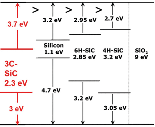


3C-SiC (Cubic Silicon Carbide)
1. Overview
3C-SiC, also known as cubic silicon carbide or β-SiC, is a wide-bandgap semiconductor within the silicon carbide (SiC) family. Unlike the common hexagonal polytypes, such as 4H-SiC and 6H-SiC, 3C-SiC has a zinc-blende cubic crystal structure. This structure provides a unique combination of properties, including high thermal conductivity, a wide bandgap, excellent electron mobility, and strong chemical stability.
At room temperature, 3C-SiC has a bandgap of about 2.36 eV. This enables outstanding performance in both electronic and optoelectronic devices. Its cubic symmetry gives the material nearly isotropic physical properties, making it ideal for high-frequency, high-power, and high-temperature applications. In addition, when grown on silicon substrates, 3C-SiC shows a lower interface trap density. This advantage has attracted significant interest in power electronics and MEMS technologies.
We also provide the sapphire wafer.

2. Structural Characteristics
 3C-SiC differs from other SiC polytypes mainly in its crystallographic structure:
Crystal Structure: Zinc-blende cubic structure
Lattice Constant: ~4.36 Å
Bandgap: ~2.36 eV
Thermal Conductivity: ~3.2 W/cm·K
Breakdown Electric Field: ~2.5 MV/cm
Electron Mobility: ~900 cm²/V·s
Hardness: Mohs ~9.2
Due to its cubic symmetry, 3C-SiC offers nearly isotropic mechanical and thermal properties, reducing crystal anisotropy issues common in hexagonal SiC wafers. This makes it an excellent material for MEMS, photonics, and quantum devices where uniform properties are essential.
3. Manufacturing and Epitaxy
3C-SiC substrates and epitaxial wafers are typically produced using one of the following techniques:
(1) Heteroepitaxy on Silicon
3C-SiC can be grown directly on silicon substrates (commonly Si (100) wafers) using chemical vapor deposition (CVD).
Advantage: Lower cost and larger wafer sizes
Challenge: Lattice mismatch (~20%) and thermal expansion differences, which can cause defects and wafer bowing
(2) Homoepitaxy on 3C-SiC Substrates
When high-quality 3C-SiC substrates are available, homoepitaxial growth yields superior crystalline quality, fewer defects, and better carrier mobility.
(3) Bulk Growth
Research on bulk 3C-SiC crystal growth is ongoing. Physical vapor transport (PVT) and sublimation epitaxy are promising techniques but are currently limited by substrate availability and cost.
4. Key Advantages
3C-SiC offers several significant advantages compared to other wide-bandgap semiconductors like GaN, 4H-SiC, and Ga2O3:
High Electron Mobility: ~900 cm²/V·s, higher than 4H-SiC, beneficial for high-speed and RF devices.
Lower Interface Trap Density: Especially on Si substrates, enabling better MOSFET performance.
Lower Thermal Barrier: Easier integration with silicon-based electronics.
Superior Mechanical Strength: High hardness and resistance to abrasion.
Excellent Chemical Stability: Resistant to acids, alkalis, and oxidation.
Optoelectronic Advantages: Suitable for UV photodetectors, LEDs, and quantum optics due to its direct bandgap properties at some wavelengths.
5. Applications
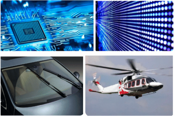 3C-SiC is increasingly adopted across multiple industries due to its versatile physical, chemical, and electronic properties:
(1) Power Electronics
MOSFETs, Schottky diodes, and IGBTs
High-voltage, high-current switching devices
Power converters for electric vehicles (EVs) and renewable energy systems
(2) Optoelectronics
Deep ultraviolet (DUV) photodetectors
Blue and green LEDs
Quantum optics and single-photon sources
(3) MEMS & Sensors
High-temperature pressure sensors
Gas sensors operating in harsh environments
Microelectromechanical systems requiring mechanical robustness
(4) Quantum Technologies
Color centers in 3C-SiC have promising properties for quantum information processing and single-photon emission.
(5) Biomedical Devices
Biocompatibility and chemical inertness make 3C-SiC suitable for implantable sensors and medical MEMS devices.
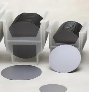
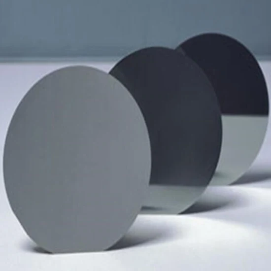
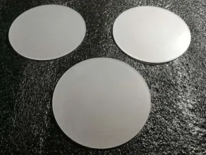
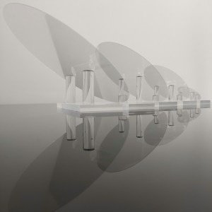
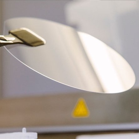
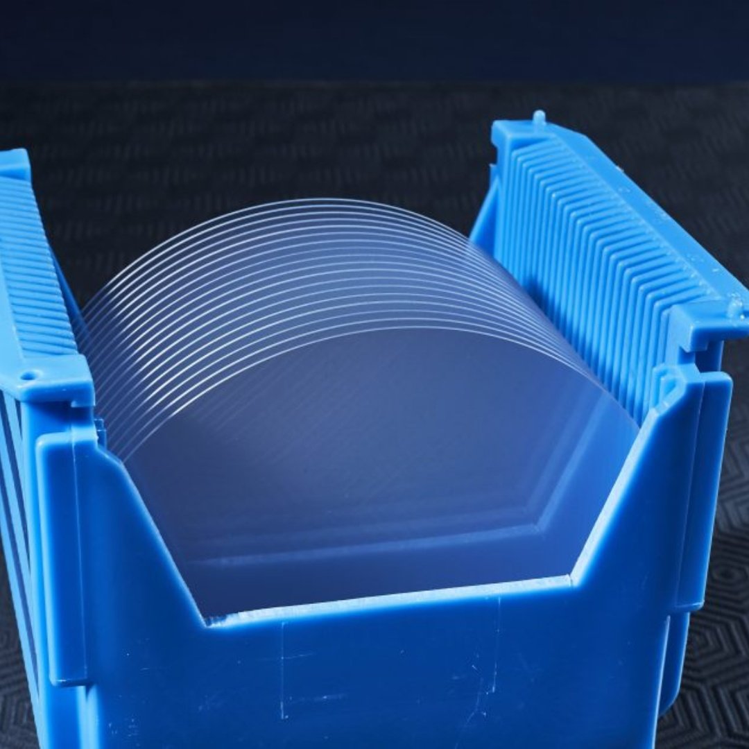
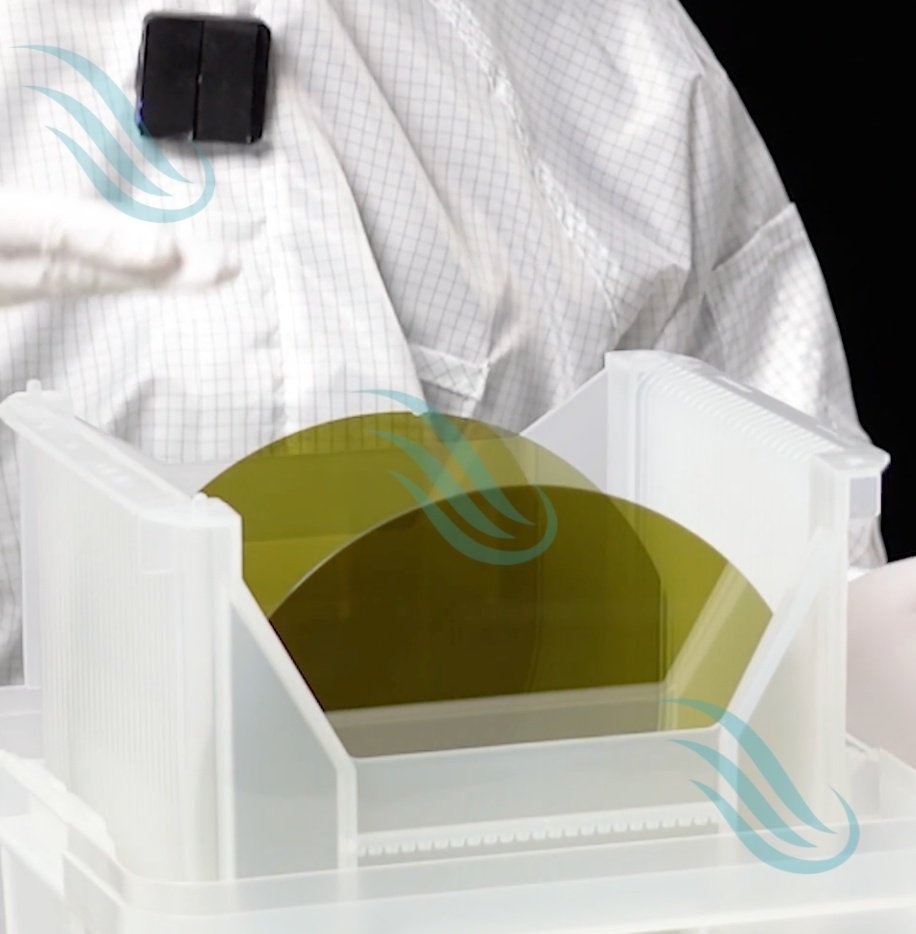
6. Product Specifications
We supply high-quality 3C-SiC wafers and epitaxial substrates with customizable specifications:
| Items | Production | Research | Dummy |
| Crystal Parameters | |||
| Polytype | 4H | ||
| Surface orientation error | <11-20 >4±0.15° | ||
| Electrical Parameters | |||
| Dopant | n-type Nitrogen | ||
| Resistivity | 0.015-0.025ohm·cm | ||
| Mechanical Parameters | |||
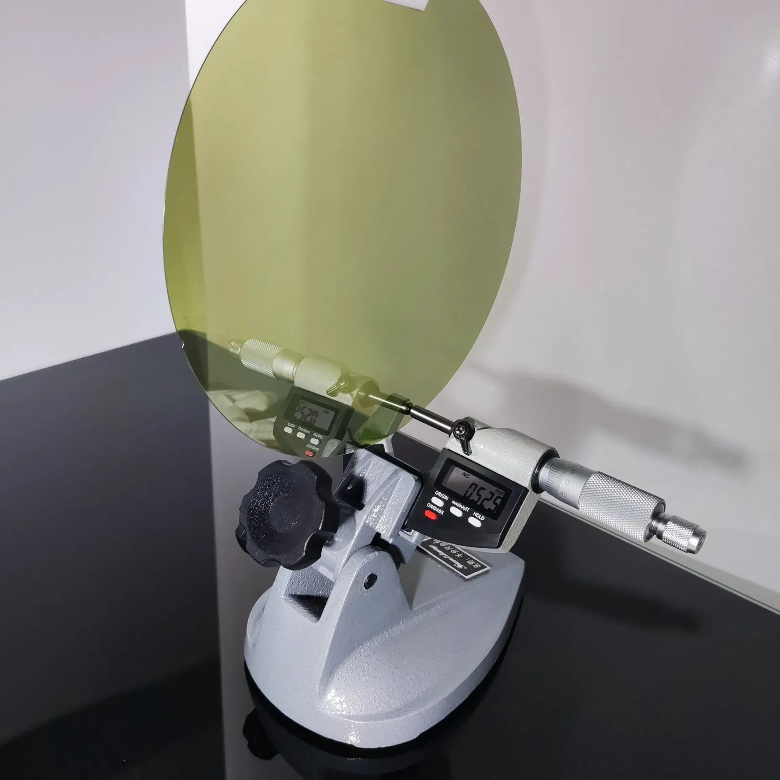
| Diameter | 150.0±0.2mm | ||
| Thickness | 350±25 μm | ||
| Primary flat orientation | [1-100]±5° | ||
| Primary flat length | 47.5±1.5mm | ||
| Secondary flat | None | ||
| TTV | ≤5 μm | ≤10 μm | ≤15 μm |
| LTV | ≤3 μm(5mm*5mm) | ≤5 μm(5mm*5mm) | ≤10 μm(5mm*5mm) |
| Bow | -15μm ~ 15μm | -35μm ~ 35μm | -45μm ~ 45μm |
| Warp | ≤35 μm | ≤45 μm | ≤55 μm |
| Front(Si-face) roughness(AFM) | Ra≤0.2nm (5μm*5μm) | ||
| Structure | |||
| Micropipe density | <1 ea/cm2 | <10 ea/cm2 | <15 ea/cm2 |
| Metal impurities | ≤5E10atoms/cm2 | NA | |
| BPD | ≤1500 ea/cm2 | ≤3000 ea/cm2 | NA |
| TSD | ≤500 ea/cm2 | ≤1000 ea/cm2 | NA |
| Front Quality | |||
| Front | Si | ||
| Surface finish | Si-face CMP | ||
| Particles | ≤60ea/wafer (size≥0.3μm) | NA | |
| Scratches | ≤5ea/mm. Cumulative length ≤Diameter | Cumulative length≤2*Diameter | NA |
| Orange peel/pits/stains/striations/ cracks/contamination | None | NA | |
| Edge chips/indents/fracture/hex plates | None | ||
| Polytype areas | None | Cumulative area≤20% | Cumulative area≤30% |
| Front laser marking | None | ||
| Back Quality | |||
| Back finish | C-face CMP | ||
| Scratches | ≤5ea/mm,Cumulative length≤2*Diameter | NA | |
| Back defects (edge chips/indents) | None | ||
| Back roughness | Ra≤0.2nm (5μm*5μm) | ||
| Back laser marking | 1 mm (from top edge) | ||
| Edge | |||
| Edge | Chamfer | ||
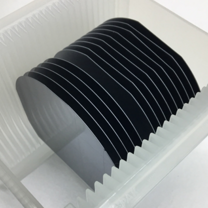
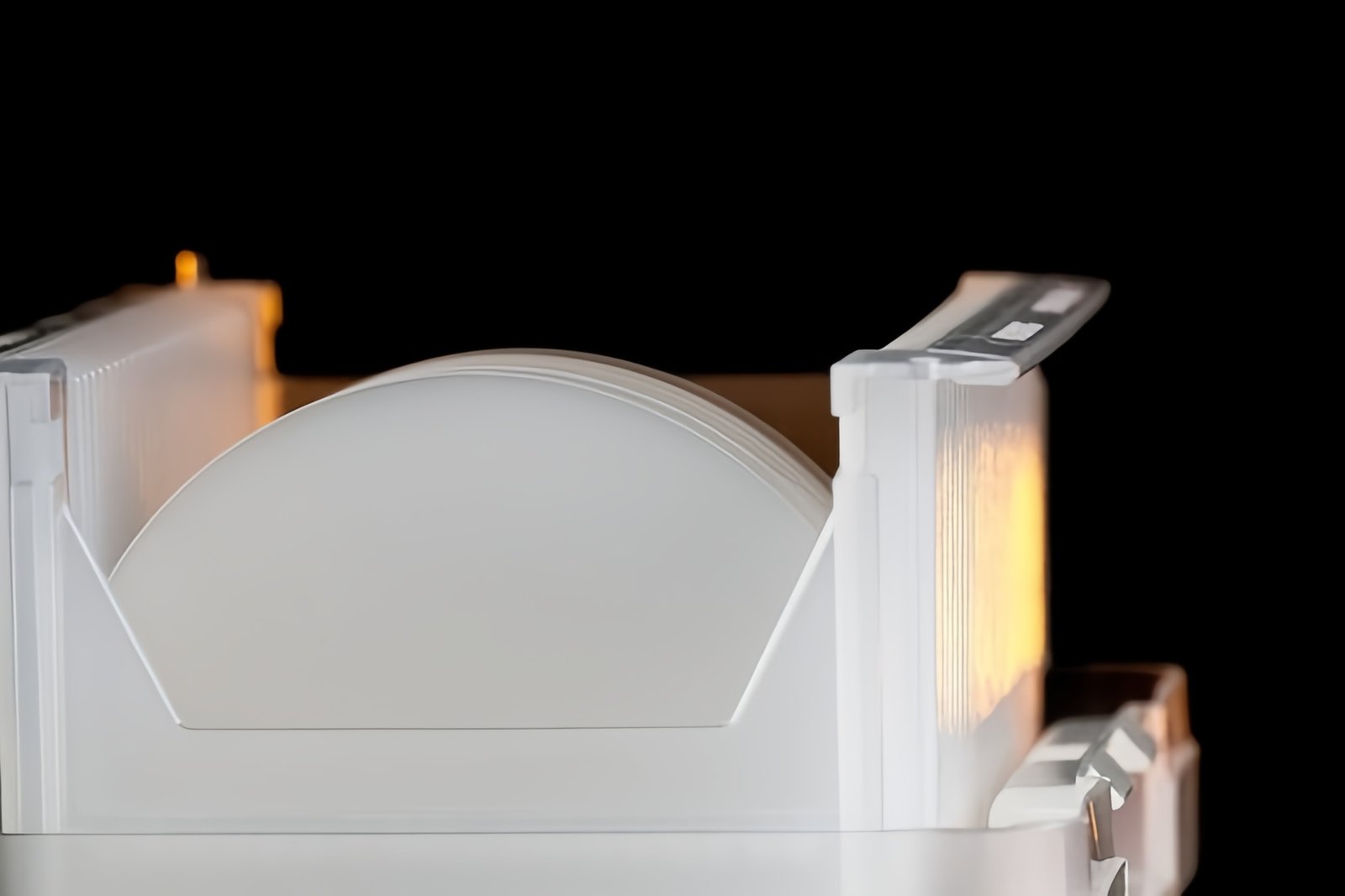
| Packaging | |||
| Packaging | Epi-ready with vacuum packaging | ||
| Multi-wafer cassette packaging | |||
| *Notes: “NA” means no request Items not mentioned may refer to SEMI-STD. | |||
7. FAQ
Q1: What is the main difference between 3C-SiC and 4H-SiC?
A1: 3C-SiC has a cubic crystal structure, while 4H-SiC is hexagonal. 3C-SiC generally provides higher electron mobility, while 4H-SiC offers higher breakdown voltage.
Q2: Can 3C-SiC be grown on silicon substrates?
A2: Yes, heteroepitaxial growth on Si is common, especially for large-diameter wafers.But careful stress management is required to minimize defects.
Q3: Is 3C-SiC suitable for high-frequency applications?
A3: Absolutely. Its high electron mobility and low interface trap density make it an excellent candidate for RF electronics.
Q4: Do you offer custom epitaxial wafers?
A4: Yes, we provide tailor-made epitaxial layers, doping concentrations, and thicknesses to meet specific research and industrial requirements.
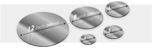
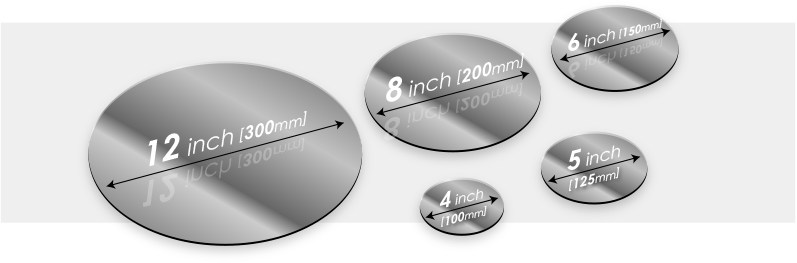
Q5: What sizes are available?
A5: Currently, 2-inch, 3-inch, and 4-inch wafers are available. Larger diameters are under development.
Pertinent Literature: 3c-sic
