


12-Inch Sapphire Wafer: Cutting-Edge Insights for Semiconductor and Optoelectronics
Introduction
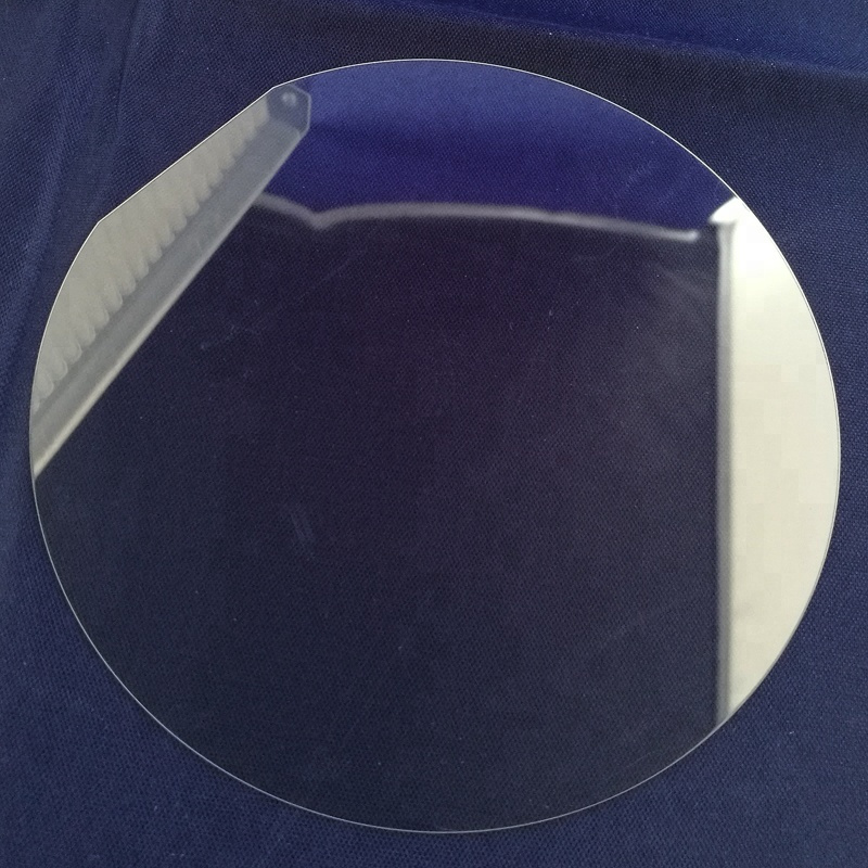
The 12-inch sapphire wafer has become a cornerstone of modern semiconductor and optoelectronic industries. As demand for more efficient and powerful devices increases, 12-inch sapphire wafers offer a critical solution due to their superior properties, including high thermal conductivity, optical clarity, and mechanical strength. In addition, these properties make the wafers essential for various high-performance applications. This article delves into the latest advancements in 12-inch sapphire wafer technology, while also addressing key questions and challenges that continue to shape the future of industries such as LED manufacturing, semiconductor fabrication, and optical device production.
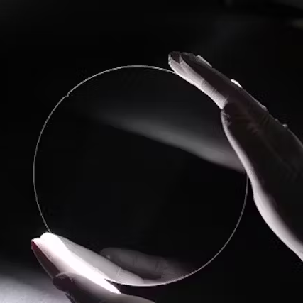
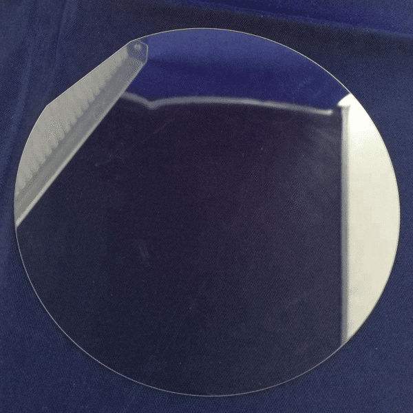
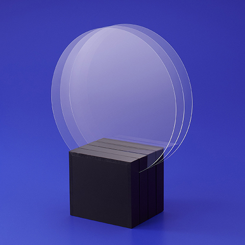
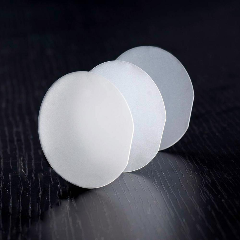
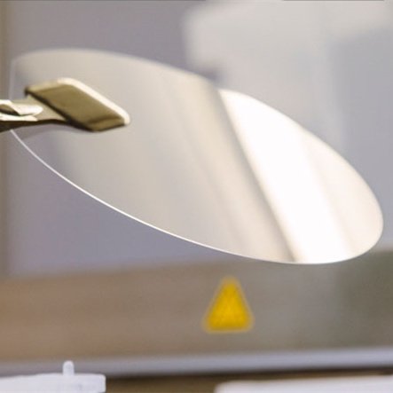
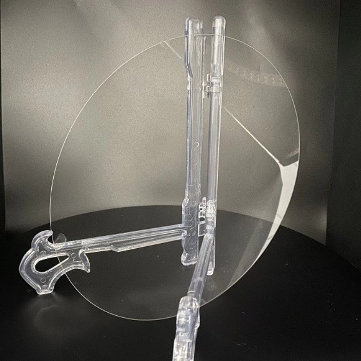
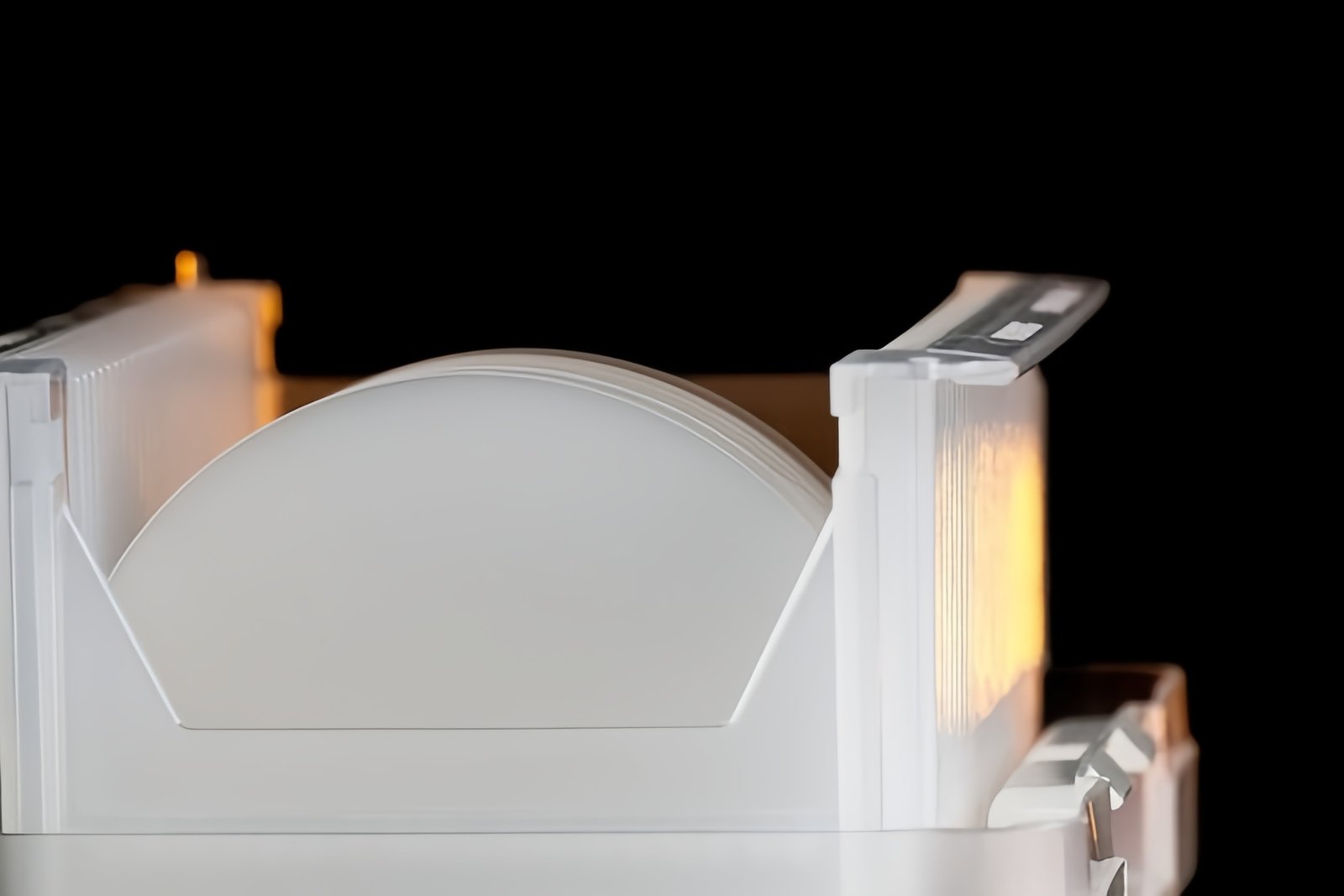
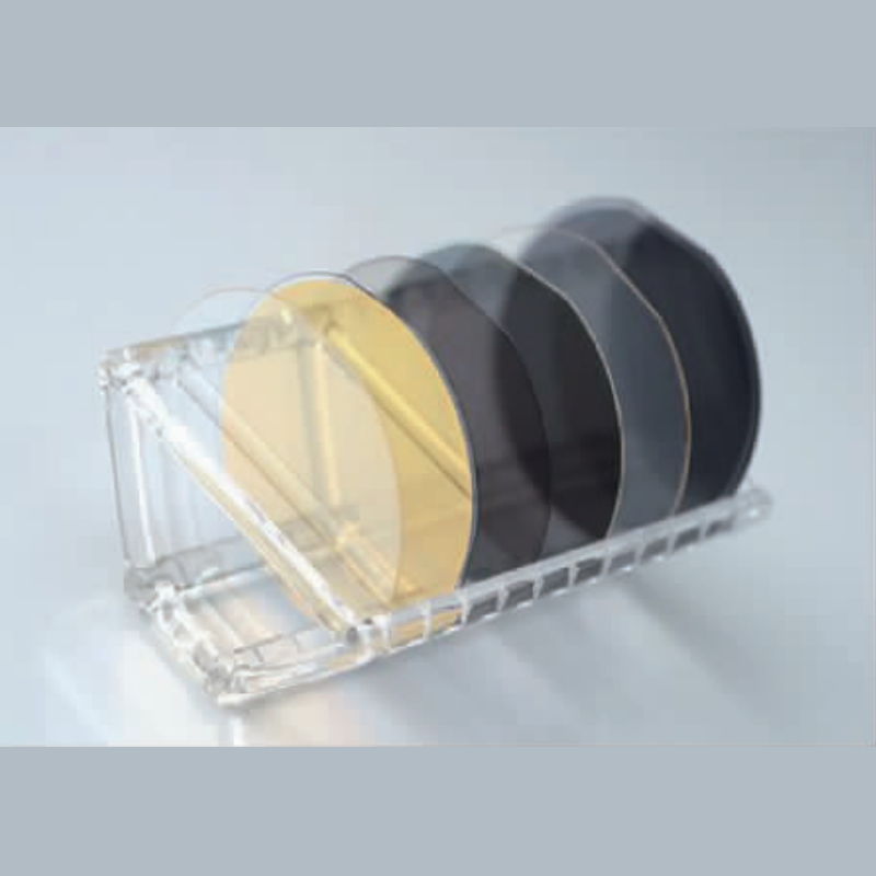
Key Specifications of the 12-Inch Sapphire Wafer
The 12-inch sapphire wafer for precision to support cutting-edge technologies. Below are the key specifications that define its role in high-performance applications:
| Parameter | Specification |
|---|---|
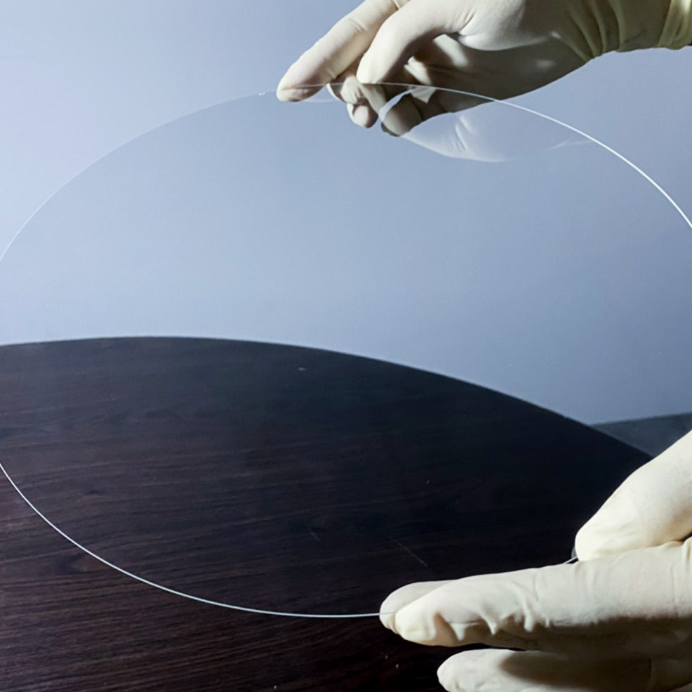
| Material | >99.99% High Purity, Mono-Crystalline AI₂O₃ |
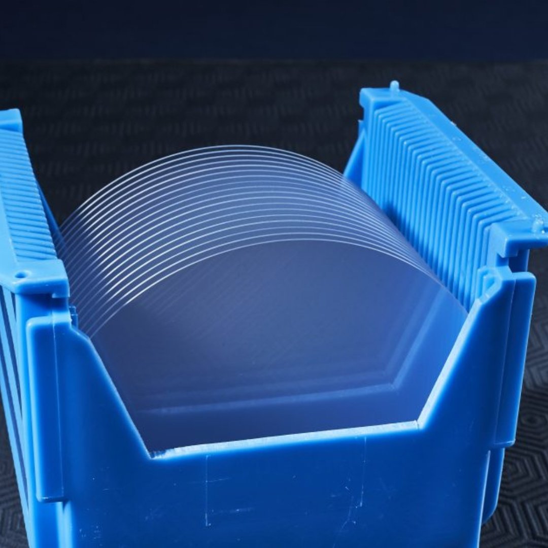
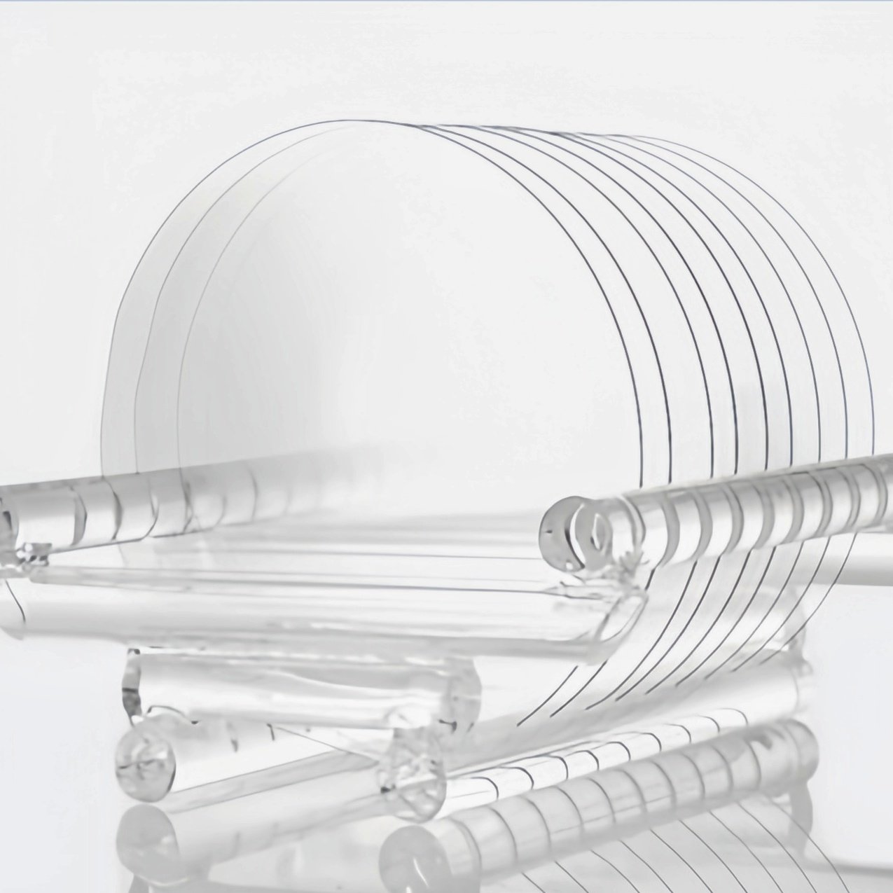
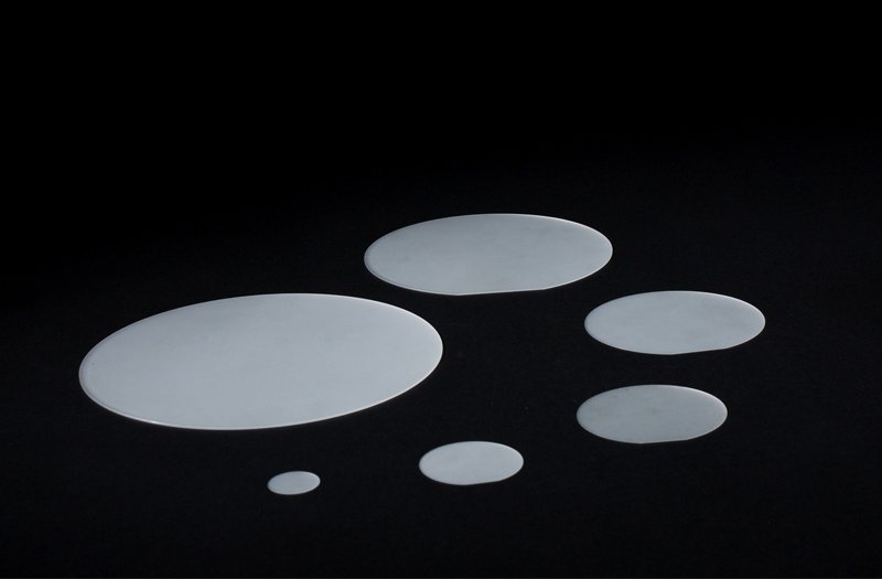
| Diameter | 12 inches (300mm ± 0.2mm) |
| Thickness | 500μm – 1500μm |
| Orientation | C-Plane (0001) |
| TTV (Total Thickness Variation) | ≤20μm |
| BOW (Wafer Curvature) | ≤30μm |
| WARP | ≤100μm |
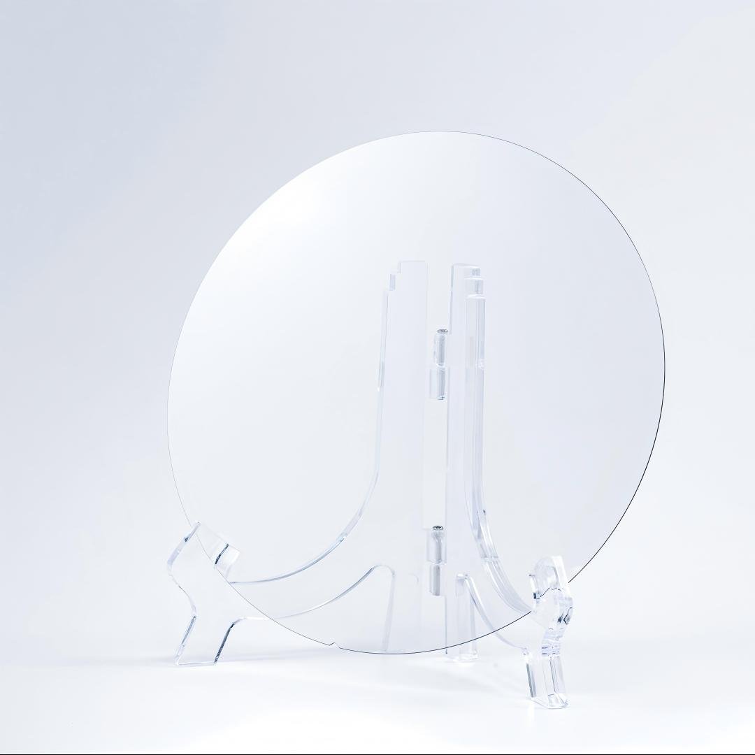
| Surface Finish | Double-Side Polished |
| Scratch & Defect Tolerance | ≤3 scratches within 2mm of the edge |
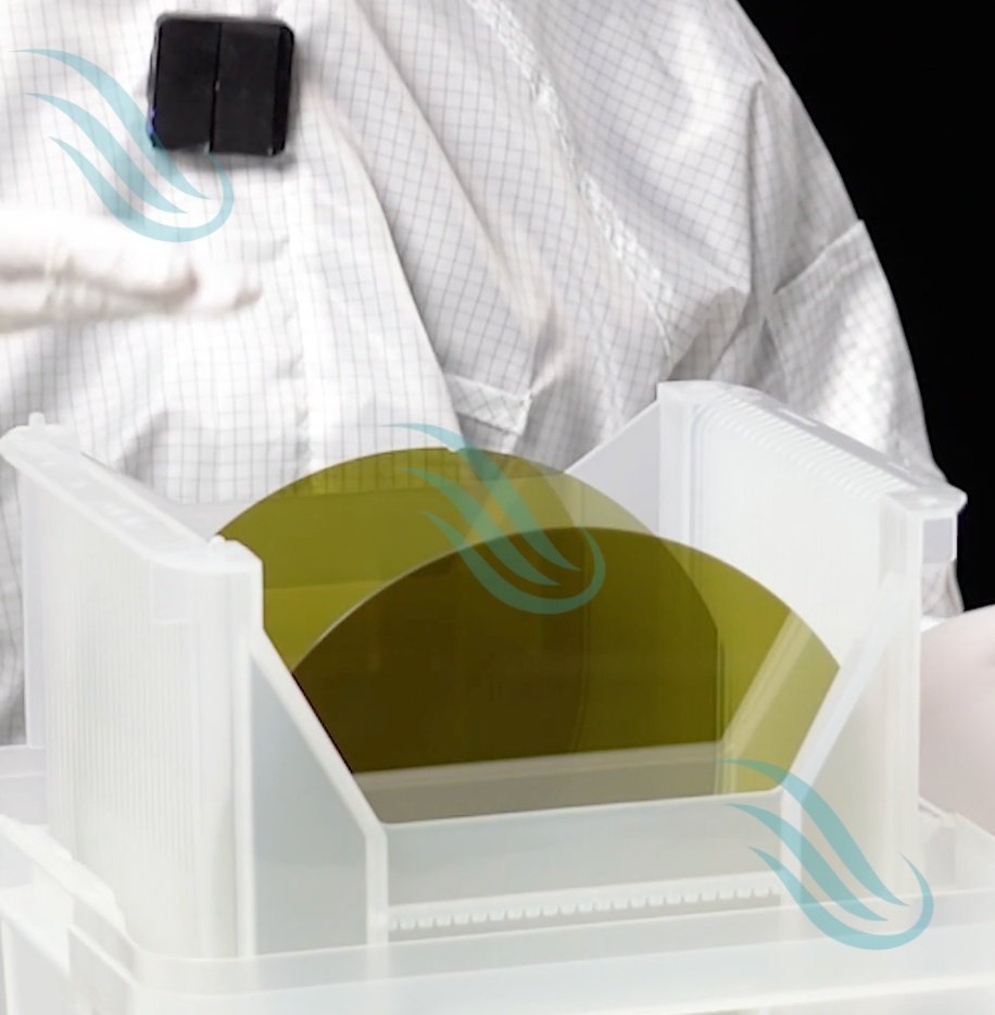
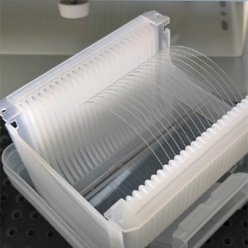
| Packaging | CRC100 packed, 1pc per box |
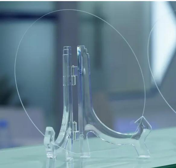
12-Inch Sapphire Wafer and Cutting-Edge Applications
The 12-inch sapphire wafer finds applications across a range of advanced industries, particularly in semiconductors and optical devices. This wafer is especially beneficial in sectors that demand high power and thermal management, such as LEDs, power electronics, and laser diodes. Additionally, its unique properties make it indispensable for these applications. Furthermore, industries that rely on precision and durability increasingly turn to 12-inch sapphire wafers. The following are some of the key sectors driving the demand for these wafers:
1. LED Manufacturing
As the LED industry grows, the 12-inch sapphire wafer has become the go-to material for high-power LEDs. The thermal conductivity of sapphire helps dissipate heat efficiently, preventing overheating in high-power LED devices. The optical properties of the sapphire also increase the light output, improving the efficiency of lighting solutions.
2. Semiconductor Industry
In the semiconductor sector, the 12-inch sapphire wafer offers both mechanical strength and electrical insulation, making it ideal for high-performance semiconductor devices. It can withstand high thermal loads, which makes it crucial for the production of devices used in high-power electronics and optical sensors.
3. Optical Devices
The optical clarity of sapphire wafers makes them the preferred choice in manufacturing optical windows, lenses, and other components used in lasers, camera modules, and display systems. Their ability to transmit light while maintaining structural integrity under stress makes them an ideal material for cutting-edge optical technologies.
Challenges in 12-Inch Sapphire Wafer Technology
As manufacturers continue to develop the 12-inch sapphire wafer, they face several technical challenges that they must address to maintain its relevance in advanced applications. These challenges include:
1. Defect Control
One of the most significant challenges in 12-inch sapphire wafer production is controlling defects, such as bubbles, scratches, and TTV (Total Thickness Variation); as a result, even slight imperfections can negatively affect the wafer’s performance, particularly in LED and semiconductor fabrication. Furthermore, as the demand for larger wafers increases, maintaining consistent quality becomes more difficult. Therefore, this requires the implementation of more advanced quality control techniques to ensure that the wafers meet the necessary standards.s.
2. Scaling Up Production
With the semiconductor industry moving towards larger wafer sizes, 12-inch sapphire wafers must continue to meet the growing demand. Scaling up production while maintaining high purity and uniformity presents a significant challenge. Manufacturers must optimize the Czochralski process, commonly used for crystal growth, to produce larger crystals with fewer defects.
3. Thermal Management
While sapphire wafers already provide excellent thermal conductivity, the continuous evolution of high-power devices demands even more advanced materials. As semiconductor devices become smaller and more powerful, efficient thermal management becomes even more crucial. 12-inch sapphire wafers must continue to evolve in this aspect to meet future demands.
The Future of 12-Inch Sapphire Wafers
Looking ahead, several technological advancements could further enhance the performance and application of the 12-inch sapphire wafer. Some of these advancements include:
1. Improved Crystal Growth Techniques
Researchers are exploring new methods to improve the Czochralski process and other crystal growth techniques. By refining these processes, manufacturers can produce larger and defect-free sapphire crystals. This improvement would significantly enhance the quality of 12-inch sapphire wafers and open the door to new applications.
2. Advanced Surface Coatings
Researchers are increasingly combining sapphire with materials like graphene to enhance its performance; in this regard, this integration could potentially improve electrical conductivity and thermal dissipation, benefiting both semiconductor and optical industries.
Furthermore, sapphire is often used as a substrate for III-V semiconductors (e.g., gallium nitride (GaN)); as a result, this highlights its versatility in advanced applications.
3. Integration with New Materials
Researchers are increasingly combining sapphire with materials like graphene to enhance its performance; therefore, this integration could potentially improve electrical conductivity and thermal dissipation, benefiting both semiconductor and optical industries. In addition, sapphire is often used as a substrate for III-V semiconductors (e.g., gallium nitride (GaN)), which consequently further highlights its versatility in advanced applications.
Frequently Asked Questions (FAQ) About the 12-Inch Sapphire Wafer
Q1: What industries use the 12-inch sapphire wafer?
A: Researchers primarily use the 12-inch sapphire wafer in the LED, semiconductor, and optical industries. It is essential for LED manufacturing, high-power semiconductors, and optical components like lenses, windows, and displays.
Q2: Why is the 12-inch sapphire wafer ideal for LED applications?
A: The 12-inch sapphire wafer is preferred for LED applications because of its thermal conductivity, which in turn allows for efficient heat dissipation in high-power LEDs. In addition, its optical clarity improves light output, therefore making LEDs more efficient and durable.
Q3: Can the 12-inch sapphire wafer be customized for specific applications?
A: Yes, manufacturers offer customization options for 12-inch sapphire wafers. These options include thickness adjustments, surface finishes, and orientation specifications to meet the specific requirements of various LED, semiconductor, and optical applications.
Q4: How does the 12-inch sapphire wafer compare to silicon wafers?
A: The 12-inch sapphire wafer offers superior thermal conductivity and optical properties, which make it ideal for high-performance applications. In contrast, silicon wafers are cheaper and more commonly used in standard electronics and semiconductors, but they lack the thermal and optical properties of sapphire.
Conclusion
The 12-inch sapphire wafer remains an essential material for the LED, semiconductor, and optical industries. As technology advances, manufacturers continue to refine the production processes of sapphire wafers to meet the increasing demands of modern high-performance applications. With its thermal conductivity, mechanical strength, and optical clarity, the 12-inch sapphire wafer will remain at the forefront of technological advancements in these sectors.
