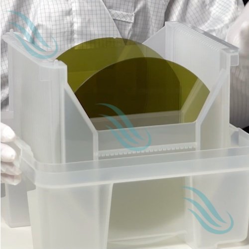
The Development of Third-Generation Semiconductor SiC wafer
The Development of Semiconductor Materials
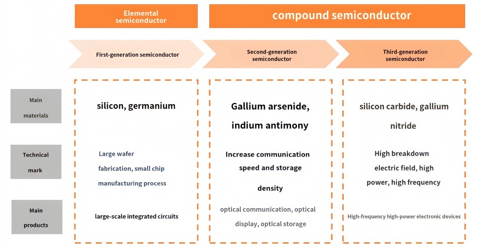
The development of semiconductor materials has gone through three major stages(SiC wafer).
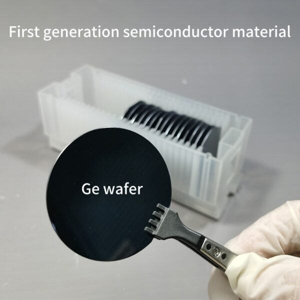
First-Generation Semiconductors
Elemental semiconductors, primarily silicon (Si) and germanium (Ge), represent the first generation.With the ability to grow large-size crystals and fabricate small chips, they enabled the rise of large-scale integrated circuits.laying the foundation for the modern electronics industry.

Ge wafer first generation semiconductor material Second-Generation Semiconductors
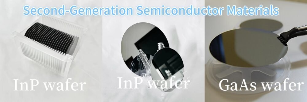
The second generation introduced compound semiconductors, such as gallium arsenide (GaAs) and indium phosphide (InP). These materials significantly improved communication speed and storage density, making them vital in optical communication, displays, and optoelectronic storage devices.
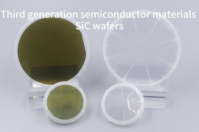
II generation semiconductor material GaAs wafer InP wafer Third-Generation Semiconductors
Wide bandgap materials, including silicon carbide (SiC) and gallium nitride (GaN), characterize the third generation.They feature high breakdown voltage, high power capability, and high-frequency performance, which are crucial for advanced power electronic devices, renewable energy systems, electric vehicles, and 5G communications.third generation semiconductor materials- SiC wafer
Overall, the transition from elemental semiconductors to wide bandgap materials reflects the continuous drive toward higher efficiency, faster communication, and greater energy sustainability.
Comparison of Key Properties of Semiconductor Materials
| Semiconductor Material | Bandgap (eV) | Breakdown Field Strength (MV/cm) | Electron Mobility (cm²/V·s) | Hole Mobility (cm²/V·s) | Thermal Conductivity (W/cm·K) |
|---|---|---|---|---|---|
| Si (First Gen.) | 1.12 | 0.3 | 1350 | 480 | 1.3 |
| GaAs (Second Gen.) | 1.43 | 0.06 | 8500 | 400 | 0.55 |
| GaN (Third Gen.) | 3.37 | 5 | 1250 | <200 | 2 |
| 4H-SiC (Third Gen.) | 3.26 | 3 | 800 | 115 | 4.9 |
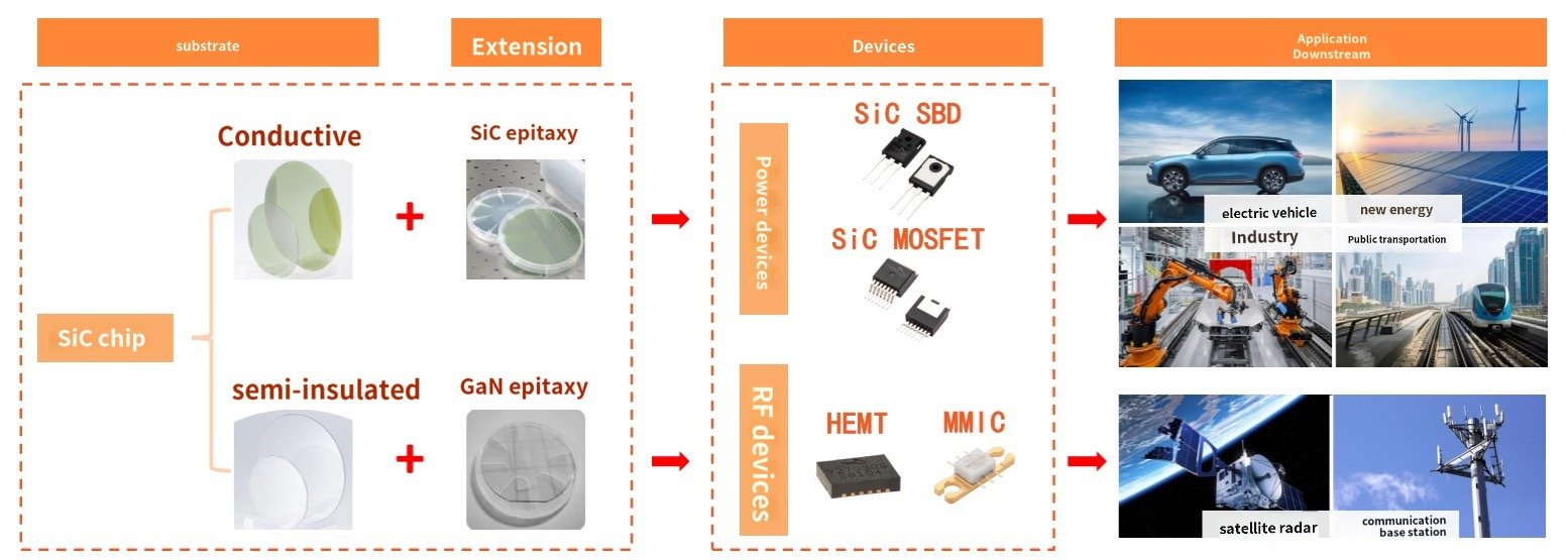
Classification and Downstream Applications of Silicon Carbide (SiC)
We categorize silicon carbide (SiC) wafers into conductive types and semi-insulating types. These wafers form the foundation for different downstream applications. Conductive SiC wafers primarily support SiC epitaxy. This process enables the fabrication of power devices such as SiC Schottky Barrier Diodes (SBDs) and SiC MOSFETs. Engineers widely apply these devices in electric vehicles, renewable energy systems, industrial automation, and rail transit. In these fields, high efficiency and high reliability are essential.
Semi-insulating SiC wafers, by contrast, often pair with GaN epitaxy. This combination produces radio-frequency (RF) devices, including HEMTs (High Electron Mobility Transistors) and MMICs (Monolithic Microwave Integrated Circuits).
hese devices are critical in satellite communications, radar systems, and telecommunication base stations, enabling high-frequency, high-power, and high-speed signal transmission.
Through this classification and application pathway, SiC plays a pivotal role in powering next-generation energy, mobility, and communication technologies.
Application Markets of SiC Wafers
1. Electric Vehicles (EVs) and Charging Infrastructure
SiC MOSFETs and Schottky diodes widely use SiC wafers to achieve higher efficiency and lower energy loss, and compact design. In EVs, they improve inverter performance more over extend driving range, and enable fast charging. In charging stations, SiC power devices allow high-voltage, high-power charging solutions.
2. Renewable Energy
In solar inverters and wind power converters, SiC devices enhance power conversion efficiency and reduce heat generation. This leads to higher energy yield and lower system costs and making SiC essential for the global transition to clean energy.
3. Industrial Applications
SiC wafers support motor drives, robotics, and industrial power supplies, enabling high efficiency and compact size, and long-term reliability. They are particularly important in smart factories and automation systems.
4. Rail Transit and Power GridRailway traction systems and smart grids, and HVDC transmission use high-power SiC devices to ensure stable, efficient, and safe energy distribution.
5. Communication and Aerospace
Engineers combine semi-insulating SiC wafers with GaN epitaxy to produce RF devices (HEMTs, MMICs).
Researchers and industry widely apply these devices in 5G base stations and radar systems, and satellite communications, where they support high frequency, high power, and low-loss signal transmission.
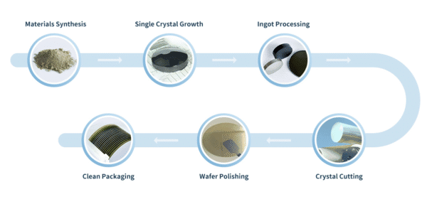
How are Silicon Carbide (SiC) wafers produced?
The production of silicon carbide (SiC) wafers involves several critical steps to ensure high crystal quality and surface precision:
Materials Synthesis – High-purity silicon and carbon sources are synthesized to form the raw material powder required for crystal growth.
Single Crystal Growth – Techniques such as the physical vapor transport (PVT) method heat the powder at high temperature and allowing a single SiC crystal (boule) to grow under controlled conditions.
Ingot Processing – Engineers process the grown SiC boule into cylindrical ingots and ensuring uniformity and eliminating crystal defects.
Crystal Cutting – The ingots are sliced into thin wafers using precision cutting equipment and usually diamond-coated wire saws.
Wafer Polishing – The wafer surfaces are carefully polished to achieve atomic-level smoothness and flatness and which is essential for epitaxy and device fabrication.
Clean Packaging – Technicians clean, inspect, and package the wafers in a contamination-free environment to meet the strict standards of semiconductor manufacturing.
Through this process, SiC wafers are produced with superior thermal conductivity, wide bandgap, and high breakdown voltage and making them ideal for power electronics, electric vehicles and renewable energy, and 5G communication devices.
Why Are Silicon Carbide (SiC) Wafers So Expensive?
The high cost of SiC wafers is mainly driven by their complex production process and the demanding requirements of advanced applications:
Challenging Crystal Growth
SiC single crystals are typically grown using the physical vapor transport (PVT) method and which requires extremely high temperatures (above 2,000 °C) and long processing times. Maintaining crystal quality and reducing defects, and producing large-diameter boules are technically difficult and energy-intensive.Difficult Wafer Processing
Unlike silicon, SiC is an ultra-hard material. Cutting and grinding, and polishing SiC wafers require diamond-based tools and advanced equipment, which increases both manufacturing time and costs.Lower Yield and Limited Supply
Due to crystal defects such as micropipes and dislocations and the yield rate of high-quality SiC wafers is relatively low. Combined with the limited number of global suppliers, this scarcity drives prices higher.High Performance and Market Demand
SiC wafers enable devices with high breakdown voltage and high power density, and high efficiency, making them indispensable for electric vehicles, renewable energy systems and 5G base stations, and aerospace applications. Growing demand from these industries further pushes up wafer prices.
| Growth Method | Growth Temperature (°C) | Growth Rate (mm/h) | Advantages | Limitations | Major Suppliers |
|---|---|---|---|---|---|
| Physical Vapor Transport (PVT) | 2200–2500 | 0.2–0.4 | Most mature and widely used | Difficult to fabricate semi-insulating substrates; thickness uniformity issues; no fully integrated equipment | Wolfspeed, Coherent, SiCrystal, TankeBlue, TYSTC |
| High-Temperature Chemical Vapor Deposition (HTPVD) | ~2200 | 0.3–1.0 | Continuous raw material supply; adjustable parameters; potential for integrated equipment | Complex process control and equipment cost | Norstel, Nippon Steel & Sumikin |
| Liquid Phase Epitaxy (LPE) | 1460–1800 | 0.5–2.0 | Similar to melt growth; relatively fast | Metal contamination; carbon precipitation; poor scalability | Showa Denko, others |
SiC Wafer Price Trend: Will They Remain Expensive in the Future?
The transition to 8-inch SiC wafers is becoming a key development trend in the semiconductor industry. Currently, the production of SiC wafers remains technically challenging, with low yield rates and high manufacturing costs, which makes SiC devices significantly more expensive compared to silicon-based products.
However, as wafer sizes increase, the number of chips that can be produced per wafer also rises. According to Wolfspeed, an 8-inch SiC wafer can accommodate 845 chips of 32 mm², compared to 448 chips on a 6-inch wafer. This represents an 89% increase in chip output. Moreover, the edge loss rate decreases from 14% on 6-inch wafers to 7% on 8-inch wafers, leading to improved efficiency.
Industry forecasts, including those from GTAT, suggest that the adoption of 8-inch SiC wafers could reduce device manufacturing costs by 20%–35%. With further optimization of production processes and the upgrading of manufacturing equipment, the cost advantages of larger wafer sizes will continue to grow.
In terms of market pricing, data shows that the price of a 6-inch conductive SiC wafer has already declined from $895 in Q1 2021 to around $770 in Q1 2023, reflecting the trend toward gradual cost reduction. Looking ahead and the industry expects that the widespread deployment of 8-inch SiC wafers will accelerate this price decline and ultimately making SiC-based devices more cost-competitive in applications such as electric vehicles, renewable energy, and industrial power systems.
SiC Wafer Price for Now(Our 8-inch SiC wafers are highly competitive in the market. We welcome your inquiries and have successfully assisted multiple companies in completing their bids. Please contact:)
The Utilization Rate of SiC Wafers in Actual Chips and How to Improve It
Engineers define the utilization rate of a SiC wafer as the effectiveness with which the wafer area produces functional chips. Factors such as wafer diameter, edge loss, and defect density influence this rate.
6-inch wafer:
Can produce 448 chips (based on a 32 mm² chip size).
The edge loss ratio is about 14% so meaning a relatively large portion of the wafer area cannot be used due to edge defects or layout limitations.
8-inch wafer:
Can produce 845 chips under the same conditions.
The edge loss ratio drops to 7%, which means a higher proportion of the wafer area is effectively utilized.
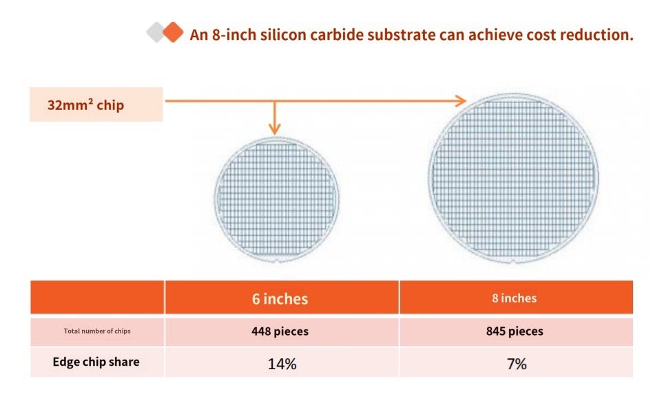
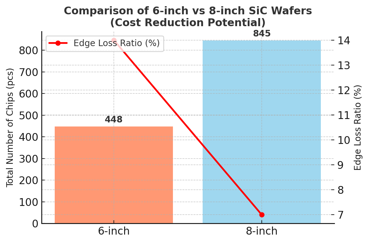
Analysis
By moving from 6-inch to 8-inch wafers, the total chip count increases by 89% while the edge loss ratio is reduced by half. This significant improvement in utilization rate directly lowers the cost per chip and enhances overall manufacturing efficiency.
Therefore, the larger wafer size not only improves material efficiency but also plays a critical role in reducing production costs and supporting the mass adoption of SiC devices in industries like EVs, renewable energy, and power electronics
At present, SiC wafers can be stably supplied in 12-inch sizes.
Current Status and Development of 12-Inch SiC Wafers
In November 2024, China’s silicon carbide substrate manufacturer SICC unveiled the industry’s first 300 mm (12‑inch) SiC substrate at Semicon Europe and marking a significant step toward ultra-large silicon carbide substrates
By March 2025, at SEMICON China and SICC further highlighted its comprehensive 12‑inch SiC offerings—ranging from high‑purity semi-insulating to P‑type and N‑type conductive substrates. The expanded product lineup demonstrated not only technological maturity in crystal growth, defect control, and processing, but also mass production readiness. SICC exhibited a 2.5× increase in chip output per wafer and reinforcing the cost-reduction advantages and signaling the industry’s firm entry into the “12‑inch era“
8-Inch SiC Wafers Take the Lead: Proven Technology, Stable Supply, and Strong Market Competitiveness
In summary, 8-inch SiC wafers are currently the most practical and competitive choice in the market. Although 12-inch SiC wafers have been introduced and their mass production capabilities are still at an early stage. Moreover, the performance stability of 12-inch products has yet to be fully verified, and their production cost remains significantly higher compared to 8-inch wafers. Therefore, at this stage, 8-inch wafers offer a more reliable and cost-effective option.
In contrast, 8-inch SiC wafers have already achieved a high level of technological maturity. Over the past years, crystal growth, wafer processing, and device fabrication techniques for 8-inch wafers have been steadily optimized. As a result, this maturity ensures consistent quality, better yields, and stable supply. Consequently and 8-inch wafers have become the mainstream solution adopted by leading manufacturers across different industries.
Looking ahead, while 12-inch wafers may gradually reduce costs and improve performance as the technology matures, 8-inch wafers will continue to dominate the market in the near term. This is because they combine proven reliability with an optimized cost-performance ratio. In addition, their wide adoption across key application sectors—such as electric vehicles, renewable energy, and power electronics—further strengthens their position as the industry’s preferred choice.
Our 8inch SiC wafer